Product Longevity
Participating products are available for a minimum of 10 years. Designated participating products developed for the automotive, telecom and medical segments are available for a minimum of 15 years.
Sign in for a personalized NXP experience.
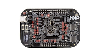
The PF1510 is a power management IC (PMIC) designed specifically for use with i.MX processors on low-power portable, smart wearable and internet-of-things (IoT) applications.
It is also capable of providing full power solution to i.MX 7ULP, i.MX 6SL, 6UL, 6ULL and 6SX processors.
With three high-efficiency buck converters, three linear regulators, DDR reference and RTC supply, the PF1510 can provide power for a complete system, including application processors, memory and system peripherals. The PF1510 is available in power efficient, space-saving 5 x 5 mm QFN package.

Participating products are available for a minimum of 10 years. Designated participating products developed for the automotive, telecom and medical segments are available for a minimum of 15 years.
1-10 of 16 results
Include 0 NRND
Part | Order | CAD Model | Status | Budgetary Price excluding tax | MCU Supported | Supply Voltage [min] (V) | Supply Voltage [max] (V) | Output Current (A) | Number of Buck Regulators | Number of LDO | Switching Frequency LV Buck (MHz) | Number of Boost Regulators | Number of Channels | IQ (μA) | Battery Charger | Package Type | Ambient Operating Temperature (Min to Max) (℃) | Safety Level | Device Function | Interface and Input Control | Additional Features - Analog | Junction Temperature (Min to Max) (℃) | Development Tools |
|---|---|---|---|---|---|---|---|---|---|---|---|---|---|---|---|---|---|---|---|---|---|---|---|
Active | 1K @ US$1.99 | Not Programmed | 2.5 | 6 | 1 | 3 | 3 | 2 | 0 | 8 | 1 | coin cell battery | HVQFN40 | -40 to 105 | QM | Ultra Low power PMIC | I2C | DDR Ref, Power Sequencing, Sleep Mode | -40 to 125 | FRDM-PF1550EVM | |||
Active | 1K @ US$1.72 | i.MX6UL, i.MX6ULL, i.MX7ULP | 2.5 | 6 | 1 | 3 | 3 | 2 | 0 | 8 | 1 | coin cell battery | HVQFN40 | -40 to 105 | QM | Ultra Low power PMIC | I2C | DDR Ref, Power Sequencing, Sleep Mode | -40 to 125 | FRDM-PF1550EVM | |||
Active | 1K @ US$1.72 | i.MX7ULP w/ LPDDR3 | 2.5 | 6 | 1 | 3 | 3 | 2 | 0 | 8 | 1 | coin cell battery | HVQFN40 | -40 to 105 | QM | Ultra Low power PMIC | I2C | DDR Ref, Power Sequencing, Sleep Mode | -40 to 125 | FRDM-PF1550EVM | |||
Active | 1K @ US$1.72 | i.MX6UL/6ULL w/ DDR3L | 2.5 | 6 | 1 | 3 | 3 | 2 | 0 | 8 | 1 | coin cell battery | HVQFN40 | -40 to 105 | QM | Ultra Low power PMIC | I2C | DDR Ref, Power Sequencing, Sleep Mode | -40 to 125 | FRDM-PF1550EVM | |||
Active | 1K @ US$1.72 | i.MX7ULP w/ LPDDR3 | 2.5 | 6 | 1 | 3 | 3 | 2 | 0 | 8 | 1 | coin cell battery | HVQFN40 | -40 to 105 | QM | Ultra Low power PMIC | I2C | DDR Ref, Power Sequencing, Sleep Mode | -40 to 125 | FRDM-PF1550EVM | |||
Active | 1K @ US$1.72 | i.MX6UL/6ULL w/ DDR3 | 2.5 | 6 | 1 | 3 | 3 | 2 | 0 | 8 | 1 | coin cell battery | HVQFN40 | -40 to 105 | QM | Ultra Low power PMIC | I2C | DDR Ref, Power Sequencing, Sleep Mode | -40 to 125 | FRDM-PF1550EVM | |||
Active | 1K @ US$1.72 | i.MX6UL/6ULL w/ DDR3L | 2.5 | 6 | 1 | 3 | 3 | 2 | 0 | 8 | 1 | coin cell battery | HVQFN40 | -40 to 105 | QM | Ultra Low power PMIC | I2C | DDR Ref, Power Sequencing, Sleep Mode | -40 to 125 | FRDM-PF1550EVM | |||
Active | 1K @ US$1.72 | i.MX6UL w LPDDR2 | 2.5 | 6 | 1 | 3 | 3 | 2 | 0 | 8 | 1 | coin cell battery | HVQFN40 | -40 to 105 | QM | Ultra Low power PMIC | I2C | DDR Ref, Power Sequencing, Sleep Mode | -40 to 125 | FRDM-PF1550EVM | |||
Active | 1K @ US$1.99 | Not Programmed | 2.5 | 6 | 1 | 3 | 3 | 2 | 0 | 8 | 1 | coin cell battery | HVQFN40 | -40 to 105 | QM | Ultra Low power PMIC | I2C | DDR Ref, Power Sequencing, Sleep Mode | -40 to 125 | FRDM-PF1550EVM | |||
Active | 1K @ US$1.92 | i.MX6UL, i.MX6ULL, i.MX7ULP | 2.5 | 6 | 1 | 3 | 3 | 2 | 0 | 8 | 1 | coin cell battery | HVQFN40 | -40 to 105 | QM | Ultra Low power PMIC | I2C | DDR Ref, Power Sequencing, Sleep Mode | -40 to 125 | FRDM-PF1550EVM |
PF1510Quick reference to our documentation types.
4 documents
Compact List
There are no results for this selection.
Sign in to access authorized secure files. Learn more about secure access rights.
Please wait while your secure files are loading.
4 documents
Compact List

Receive the full breakdown. See the product footprint and more in the eCad file.
1 hardware offering

Sign in to access authorized secure files. Learn more about secure access rights.
1 hardware offering

Quick reference to our software types.
2 software files
Note: For better experience, software downloads are recommended on desktop.
Sign in to access authorized secure files. Learn more about secure access rights.
Please wait while your secure files are loading.
2 software files
Note: For better experience, software downloads are recommended on desktop.
3 engineering services


There are no results for this selection.
There are no results for this selection.
To find additional partner offerings that support this product, visit our Partner Marketplace.
There are no recently viewed products to display.
View or edit your browsing history
Help us improve your experience on our site. We invite you to take our five-question survey.