
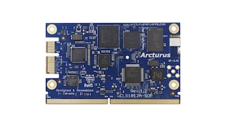
Layerscape® 1012A Low Power Processor
The VR5100 is a high performance, multi-output DC-DC regulator designed to power single or dual core LS1 processors like LS1012A and LS1024A. It includes three buck regulators, six LDOs and a boost regulator offering a complete power management solution for Network Attached Storage, battery operated Mobile NAS, IoT gateway, Home and factory automation systems.
The VR5100 uses a low quiescent current architecture allowing high efficiency operation at light load extending the battery life. The high frequency operation reduces the total solution to less than 0.5 sqin. The high power QFN package keeps the junction temperature low even at high ambient temperature.

Note: To see the product features close this window.
|
|
|
|
|
|
|
|---|---|---|---|---|---|
|
|
|
|
|
|
|
|
|
|
|
|
|
|
|
|
|
|
|
|
|
|
|
|
|
|
|
|
|
|
|
|
|
|
|
|
|
|
|
|
|
|
|
|
|
|
|
|
|
|
|
|
|
|
|
|
|
|
|
|
|
|
|
|
|
|
|
|
|
|
Quick reference to our documentation types.
1-5 of 6 documents
Please wait while your secure files are loading.
Receive the full breakdown. See the product footprint and more in the eCad file.

Receive the full breakdown. See the product footprint and more in the eCad file.
4 hardware offerings
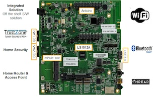
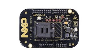
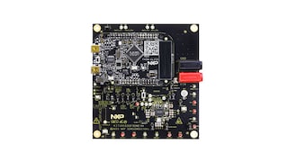
Additional hardware available. View our featured partner solutions.
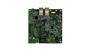
1 hardware offering
To find additional partner offerings that support this product, visit our Partner Marketplace.
1 engineering service

There are no results for this selection.
To find additional partner offerings that support this product, visit our Partner Marketplace.
1 trainings