BYLink System Power Platform
This platform facilitates the design of safe power management systems thanks to a portfolio of configurable and linkable devices. It simplifies complex power supply subsystems into a single smart solution.
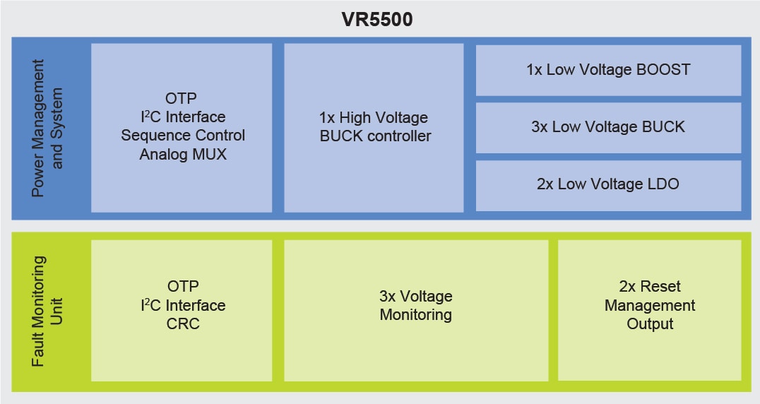
The VR55 is an automotive high voltage multi-output power supply integrated circuit, with focus on radio, telematics and infotainment applications. It includes multiple switch mode and linear voltage regulators.
This PMIC is part of a complete family of devices offering scalability in power and safety FS84 (ASIL B) and FS85 (ASIL D), pin to pin and software compatible.
| Part number | Buck 1 | Buck 2 | Buck 3 | Vpre | Boost | Safety level |
|---|---|---|---|---|---|---|
| VR5500 | 0.8 V - 1.8 V 2.5 A Multi-phase and SVS option |
12 / 24 V HV BUCK - 10 A |
5 V - 5.74 V 1.5 A peak |
Quality Mgt (QM) | ||
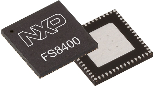
| FS8400 | N/A | N/A | Fit for ASIL B | |||
| FS8500 | Fit for ASIL D | |||||
| FS5502 | 1.0 V - 4.1 V 3.6 A peak |
N/A | Quality Mgt (QM) | |||
| FS8410 | 5 V - 5.74 V 1.5 A peak |
Fit for ASIL B | ||||
| FS8510 | Fit for ASIL D | |||||
| FS8420 | 0.8 V - 1.8 V 2.5 A Multi-phase and SVS option |
N/A | Fit for ASIL B | |||
| FS8520 | Fit for ASIL D | |||||
| FS8430 | 1.0 V - 3.3 V 2.5 A |
Fit for ASIL B | ||||
| FS8530 | Fit for ASIL D | |||||
| FS6600 | Fit for ASIL D |
This platform facilitates the design of safe power management systems thanks to a portfolio of configurable and linkable devices. It simplifies complex power supply subsystems into a single smart solution.
| | | | | |
|---|---|---|---|---|---|
| | | | | |
| | | | | |
| | | | | |
| | | | | |
| | | | | |
| | | | | |
| | | | | |
| | | | | |
| | | | | |
| | | | | |
Quick reference to our documentation types.
5 documents
Compact List
5 documents
Compact List
1 design file
2 hardware offerings
Quick reference to our software types.
1 software file
Note: For better experience, software downloads are recommended on desktop.
There are no recently viewed products to display.