Digital Absolute Pressure Sensor (20 to 550 kPa)
As of February 2, 2026, NXP MEMS sensor products have been transitioned to STMicroelectronics. For more information, contact STMicroelectronics.
NXLS95xxxx and NXLS96xxxx are the recommended devices for new designs starting Q1-2026. FXLS90xxxx and FXLS93xxxx will continue to be supported in production until inventory depletion.
The FXLS90 family is the latest generation of airbag crash sensors from NXP.
The devices are designed using NXP proprietary UMEMS sensing technology combined with a signal conditioning ASIC in a QFN 4 x 4 x 1.45 mm package.
The devices feature a user selectable DSI3 interface, 32-bit SPI interface. They can measure acceleration in single or dual independent axis configuration from +/-15.5 g to +/-500 g. The embedded DSP provides fully programmable digital high and low pass filtering.
The FXLS90 family is fully AEC-Q100 qualified up to 125 °C operating temperature and is compliant with the AK LV 27 requirements. The package has wettable flanks for solder join inspection. FXLS90 products have been developed following ISO26262 2018 edition and can be used in up to ASIL D system.
For additional information and sample availability, contact your local sales office.
Choose a diagram:

Note: To see the product features close this window.
| Discontinued Part Number | Replacement Orderable Part Number | Acceleration Range | Number of Axis | Sensing Axis | Communication Protocol | Operating Temperature |
|---|---|---|---|---|---|---|
| FXLS90120AE(S/B) | NXLS95120AES | 15.5-150 g | 1 | Z | SPI/DSI3 | -40 to +125 °C |
| FXLS90130AE(S/B) | NXLS95130AES | 50-500 g | 1 | Z | SPI/DSI3 | -40 to +125 °C |
| FXLS90220AE(S/B) | NXLS95220AES | 15.5-150 g | 1 | X | SPI/DSI3 | -40 to +125 °C |
| FXLS90230AE(S/B) | NXLS95230AES | 50-500 g | 1 | X | SPI/DSI3 | -40 to +125 °C |
| FXLS90620AE(S/B) | NXLS95620AES | 15.5-150 g | 1 | Y | SPI/DSI3 | -40 to +125 °C |
| FXLS90630AE(S/B) | NXLS95630AES | 50-500 g | 1 | Y | SPI/DSI3 | -40 to +125 °C |
| FXLS90322AE(S/B) | NXLS95322AES | 15.5-150 g | 2 | XY | SPI/DSI3 | -40 to +125 °C |
| FXLS90333AE(S/B) | NXLS95333AES | 50-500 g | 2 | XY | SPI/DSI3 | -40 to +125 °C |
| FXLS90422AE(S/B) | NXLS95422AES | 15.5-150 g | 2 | XZ | SPI/DSI3 | -40 to +125 °C |
| FXLS90433AE(S/B) | NXLS95433AES | 50-500 g | 2 | XZ | SPI/DSI3 | -40 to +125 °C |
| FXLS90722AE(S/B) | NXLS95722AES | 15.5-150 g | 2 | YZ | SPI/DSI3 | -40 to +125 °C |
| FXLS90733AE(S/B) | NXLS95733AES | 50-500 g | 2 | YZ | SPI/DSI3 | -40 to +125 °C |
| FXLS90421AE(S/B) | NXLS95421AES |
X-Axis : 15.5-150 g
Z-Axis : 1.5 - 24 g |
2 | XZ | SPI/DSI3 | -40 to +125 °C |

Digital Absolute Pressure Sensor (20 to 550 kPa)

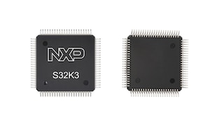
S32K3 Microcontrollers for Automotive General Purpose

Dual DSI3 Leader Transceiver for Automotive Applications

Analog Absolute Pressure Sensor (20 to 550 kPa)
|
|
|
|
|
|
|
|---|---|---|---|---|---|
|
|
|
|
|
|
|
|
|
|
|
|
|
|
|
|
|
|
|
|
|
|
|
|
|
|
|
|
|
|
|
|
|
|
|
|
|
|
|
|
|
|
|
|
|
|
|
|
|
|
|
|
|
|
|
|
|
|
|
|
|
|
|
|
|
|
|
|
|
|
Quick reference to our documentation types
6 documents
Compact List
Please wait while your secure files are loading.
Receive the full breakdown. See the product footprint and more in the eCad file.

Receive the full breakdown. See the product footprint and more in the eCad file.
2 hardware offerings


1 engineering service

There are no results for this selection.
To find additional partner offerings that support this product, visit our Partner Marketplace.