

Design Files
Receive the full breakdown. See the product footprint and more in the eCad file.
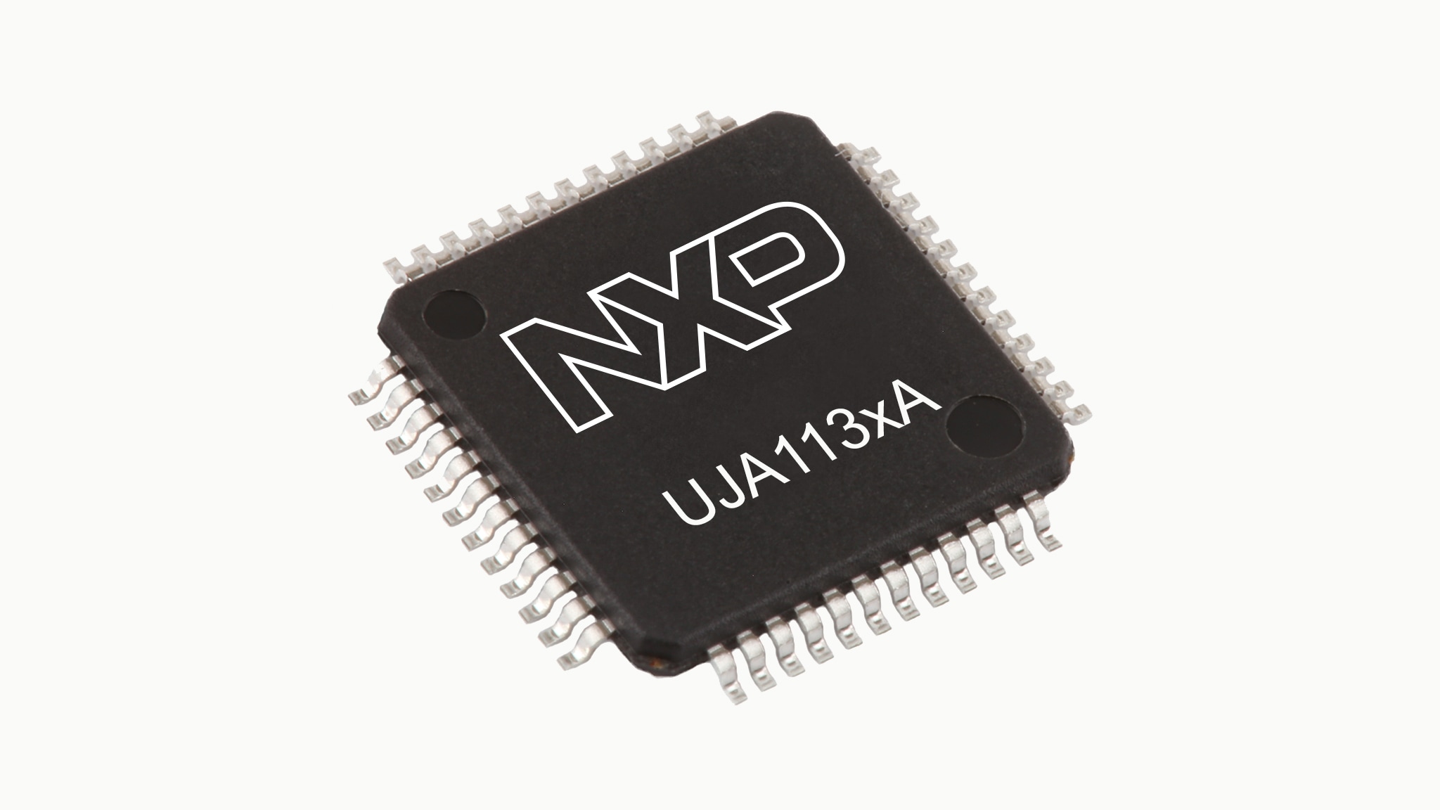
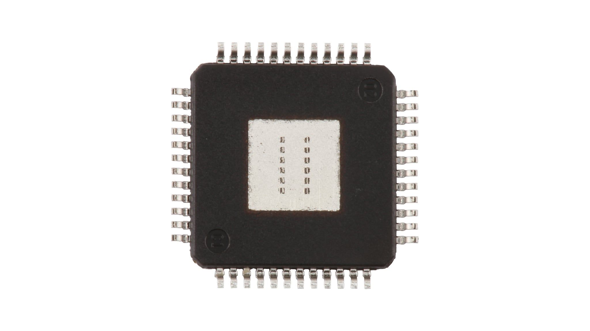
The UJA113xA System Basis Chip (SBC) contains a fully integrated automatic SMPS Buck-Boost converter, a High-Speed CAN transceiver and up to two LIN transceivers along with a number of features commonly found in typical automotive Electronic Control Units (ECUs). It interfaces directly with CAN and LIN bus lines, supplies the microcontroller, handles input and output signals and supports fail-safe features including a watchdog and advanced 'limp home' functionality configurable via non-volatile memory.
The UJA113xA implements the High-Speed CAN physical layer as defined in the ISO 11898-2:2016 standard with additional timing parameters included, defining loop delay symmetry for CAN FD communication up to 5 Mbit/s. The UJA113xAHW/xFx variants support ISO 11898-2:2016 compliant CAN partial networking with a selective wake-up function incorporating CAN FD-passive.
Choose a diagram:
| Part Number | Description | CAN PHY | LIN PHY | Safety Level | Interface and Input Control | Additional Features - Analog | AEC-Q100 Temperature Range | Ambient Operating Temperature (Min to Max) (°C) |
|---|---|---|---|---|---|---|---|---|
| UJA1131AHW | Buck/boost HS-CAN/LIN system basis chip, 5 V/500 mA + 5 V/100 mA, up to 8 HVIO, optional CAN Partial Networking | 1, CAN FD | 1 | QM | SPI | 8x HVIO, LDO (5 V/500 mA), Sensor Supply (5 V/100 mA), LIMP output, Watchdog | Grade 1 | -40 to 125 |
| UJA1132AHW | Buck/boost HS-CAN/dual-LIN system basis chip, 5 V/500 mA + 5 V/100 mA, up to 8 HVIO, optional CAN Partial Networking | 1, CAN FD | 2 | QM | SPI | 8x HVIO, LDO (5 V/500 mA), Sensor Supply (5 V/100 mA), LIMP output, Watchdog | Grade 1 | -40 to 125 |
| UJA1135AHW | Buck HS-CAN/LIN system basis chip, 5 V/500 mA + 5 V/100 mA, 8 HVIO | 1, CAN FD | 1 | QM | SPI | 8x HVIO, LDO (5 V/500 mA), Sensor Supply (5 V/100 mA), LIMP output, Watchdog | Grade 1 | -40 to 125 |
| UJA1136AHW | Buck HS-CAN/dual-LIN system basis chip, 5 V/500 mA + 5 V/100 mA, 8 HVIO | 1, CAN FD | 2 | QM | SPI | 8x HVIO, LDO (5 V/500 mA), Sensor Supply (5 V/100 mA), LIMP output, Watchdog | Grade 1 | -40 to 125 |
|
|
|
|
|
|
|
|---|---|---|---|---|---|
|
|
|
|
|
|
|
|
|
|
|
|
|
|
|
|
|
|
|
|
|
|
|
|
|
|
|
|
|
|
|
|
|
|
|
|
|
|
|
|
|
|
|
|
|
|
|
|
|
|
|
|
|
|
|
|
|
|
|
|
|
|
|
|
|
|
|
|
|
|
Quick reference to our documentation types.
Receive the full breakdown. See the product footprint and more in the eCad file.
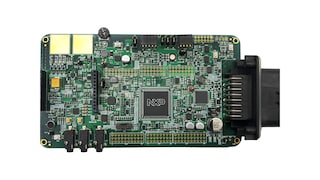
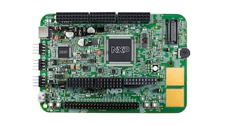
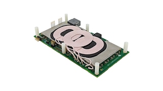
3 hardware offerings