
Product Longevity
Participating products are available for a minimum of 10 years. Designated participating products developed for the automotive, telecom and medical segments are available for a minimum of 15 years.
The NX20P5090 is an advanced 5.0 A Uni-directional power switch for USB PD. It includes under voltage lockout, over voltage lockout, reverse current protection and over-temperature protection circuits, it is designed to automatically isolate the power switch terminals when a fault condition occurs. Both VBUS and VINT pin have 29 V tolerance in shutdown mode, two NX20P5090s can be used in parallel to support dual power inputs connecting to same charging circuit.
The device has a default 23 V over voltage protection threshold, and the OVP threshold can be adjusted by using external resistors on OVLO pin. A 15 ms debounce time is deployed every time before the device is switched ON, followed by a soft start to limit the inrush current.
Designed for operation from 2.5 V to 20.0 V, it is used in USB PD power domain isolation applications to offer essential protection and enhance reliability.
NX20P5090 is offered in a small 15 bumps 1.6 × 2.6 mm, 0.5 mm pitch WLCSP package.
Participating products are available for a minimum of 10 years. Designated participating products developed for the automotive, telecom and medical segments are available for a minimum of 15 years.
| | | | | |
|---|---|---|---|---|---|
| | | | | |
| | | | | |
| | | | | |
| | | | | |
| | | | | |
| | | | | |
| | | | | |
| | | | | |
| | | | | |
| | | | | |
Quick reference to our documentation types.
3 documents
Compact List
3 documents
Compact List

Receive the full breakdown. See the product footprint and more in the eCad file.
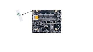
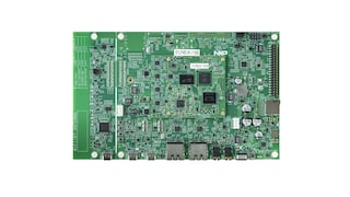
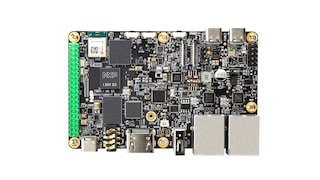
3 hardware offerings
To get further assistance directly from NXP, please see our Engineering Services.
1 engineering service

To find additional partner offerings that support this product, visit our Partner Marketplace.
There are no recently viewed products to display.