
Product Longevity
Participating products are available for a minimum of 10 years. Designated participating products developed for the automotive, telecom and medical segments are available for a minimum of 15 years.
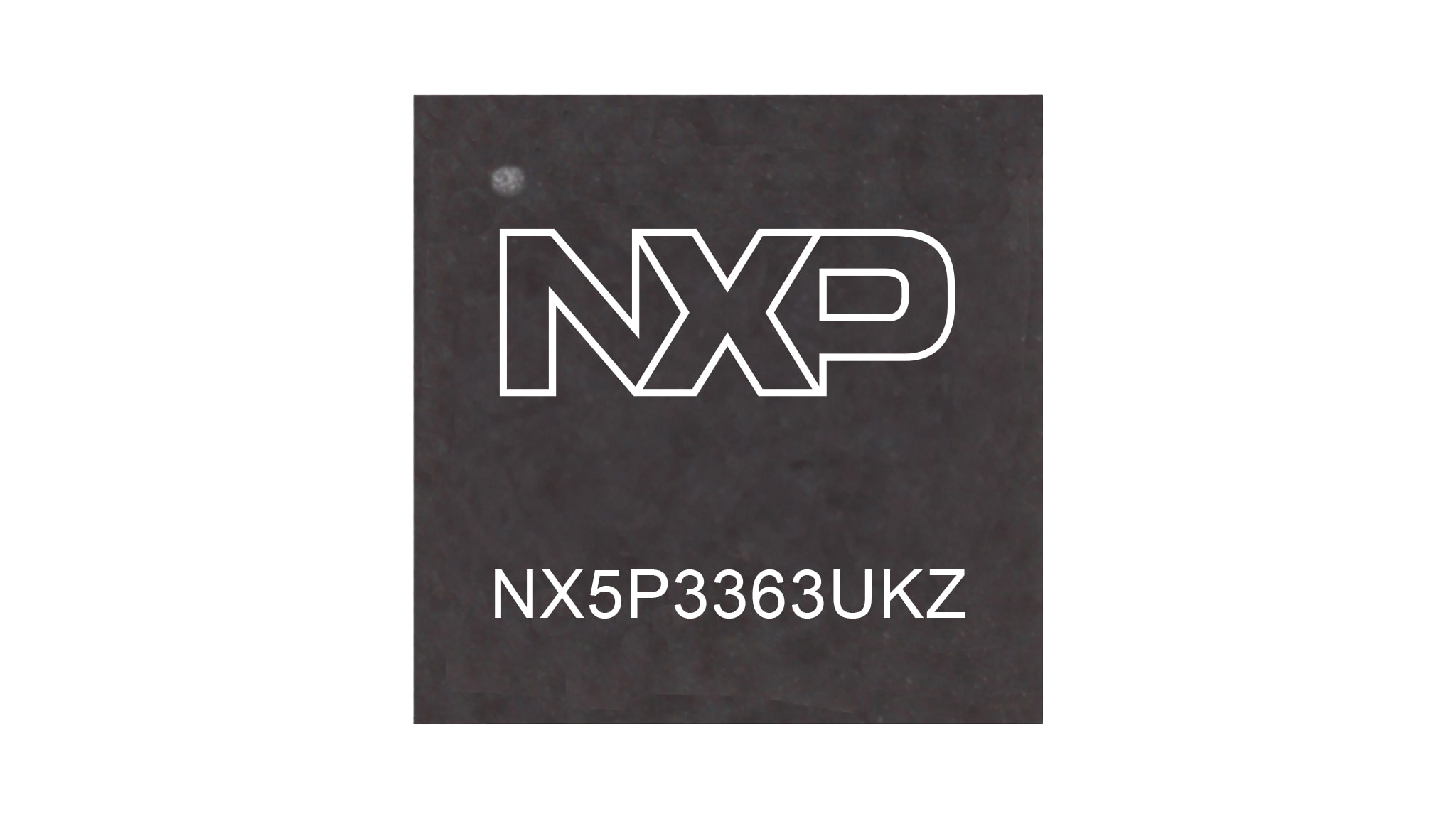
The NX5P3363 is a precision adjustable current-limited power switch for USB PD application. The device includes under voltage lockout, over-temperature protection, and reverse current protection circuits to automatically isolate the switch terminals when a fault condition occurs. The 29 V tolerance on VBUS pin ensures the device is able to work on a USB PD port; a current limit input (ILIM) pin defines the over-current limit threshold; an open-drain fault output (FLT) indicates when a fault condition has occurred.
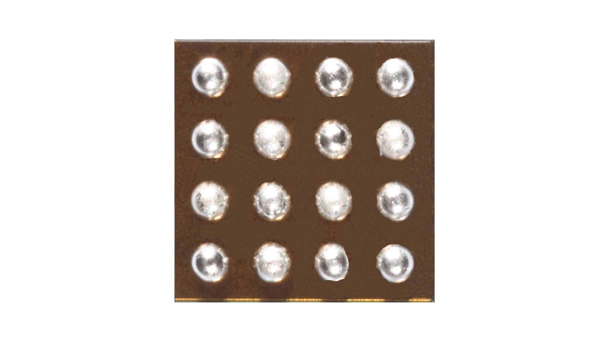
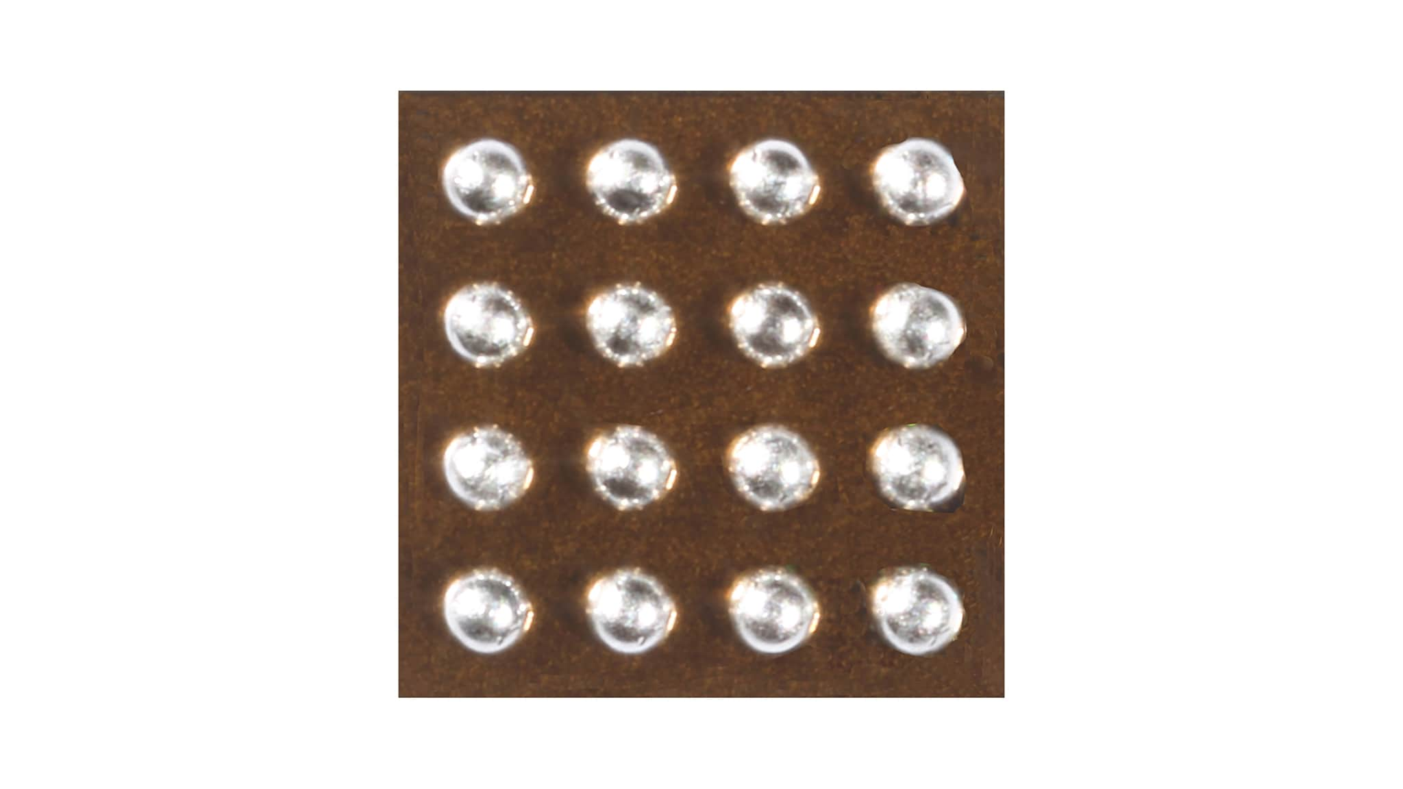
The over-current limit threshold can be programmed from 400 mA to 3.3 A, using an external resistor between the ILIM pin and GND pin. In the overcurrent condition, the device will clamp the output current to the value set by ILIM and keep the switch on while asserting the FLT flag. To minimize current surges during normal turn on, the device has built-in soft start by limiting the power switch turn-on slew rate. However, the user can disable the soft start and request a fast output by pulling FO pin HIGH. A fast RCP recovery circuit has been added to the switch to prevent reverse current flowing back to the power source at all times. When exiting from reverse current protection state, the power MOSFET will turn on within 50 us. The fast RCP recovery ensures the voltage on VBUS doesn’t drop too much in a power source swap application. NX5P3363 is offered in a 2.2 x 2.2 mm, 16 bump WLCSP package.
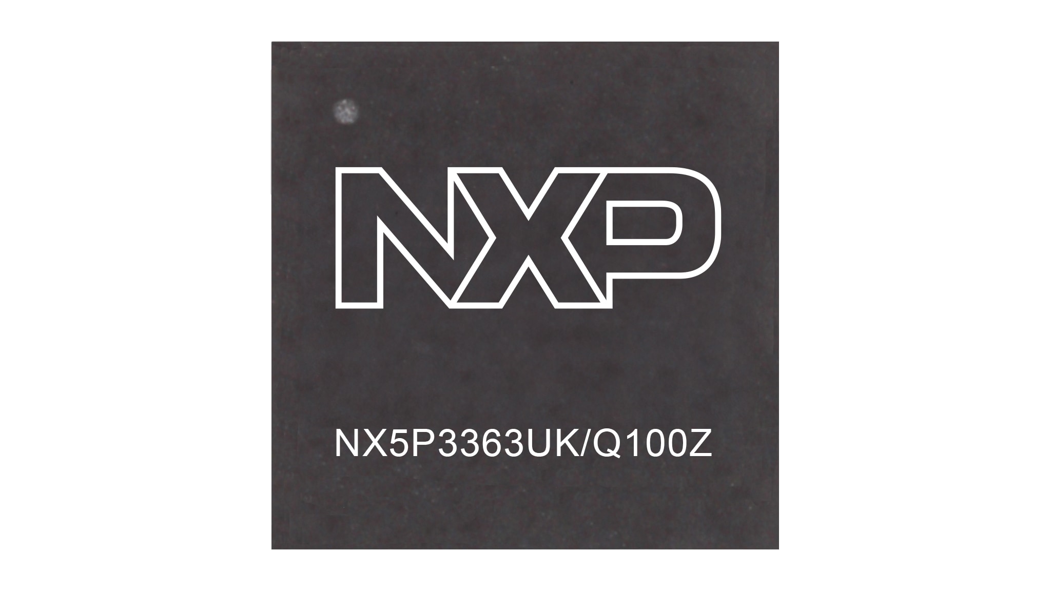
The NX5P3363UK also provides the auto-grade derivative part for automotive applications, named as NX5P3363UK/Q100Z.
| Orderable part | Market |
|---|---|
| NX5P3363UKZ | Consumer, Industrial |
| NX5P3363UK/Q100Z | Automotive |
Participating products are available for a minimum of 10 years. Designated participating products developed for the automotive, telecom and medical segments are available for a minimum of 15 years.
| | | | | |
|---|---|---|---|---|---|
| | | | | |
| | | | | |
| | | | | |
| | | | | |
| | | | | |
| | | | | |
| | | | | |
| | | | | |
| | | | | |
| | | | | |
Quick reference to our documentation types.
4 documents
Compact List
4 documents
Compact List

Receive the full breakdown. See the product footprint and more in the eCad file.
To get further assistance directly from NXP, please see our Engineering Services.
1 engineering service

To find additional partner offerings that support this product, visit our Partner Marketplace.
There are no recently viewed products to display.
