High-Voltage USB PD Power Switch
Design Files

Receive the full breakdown. See the product footprint and more in the eCad file.
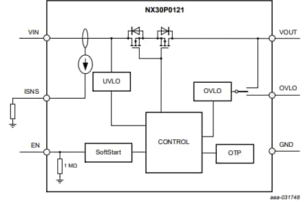
The NX30P0121UK is an advanced 3 A power switch. It includes UnderVoltage LockOut (UVLO), VOUT OverVoltage LockOut (OVLO), OVLO adjustable pin, and over-temperature protection circuits. It is designed to automatically isolate the power switch terminals when a fault condition occurs. Both VIN and VOUT pins have 29 V tolerance in shutdown mode.
The device has a default internal 14.5 V overvoltage protection threshold in VOUT and adjustable OVP threshold by resistor divider from VOUT. ISNS pin is current source output proportional to input current from VIN to VOUT when the device is enabled.
The device is enabled by external EN pin. When EN pin is driven LOW, the device is in shutdown mode where all internal circuitries are off and OVP switch is off. When EN pin is driven HIGH and VIN is valid, the OVP switch soft starts after VIN debounce time to limit the inrush current.
NX30P0121UK is offered in a small 12 bumps, 1.65 x 1.25 x 0.525 mm WLCSP package.
High-Voltage USB PD Power Switch
| | | | | |
|---|---|---|---|---|---|
| | | | | |
| | | | | |
| | | | | |
| | | | | |
| | | | | |
| | | | | |
| | | | | |
| | | | | |
| | | | | |
| | | | | |
Quick reference to our documentation types.
3 documents
Compact List
3 documents
Compact List
Receive the full breakdown. See the product footprint and more in the eCad file.
1 hardware offering
There are no recently viewed products to display.