2110-2170 MHz, 33 W Avg., 28 V Single W-CDMA Lateral N-Channel RF Power MOSFETs

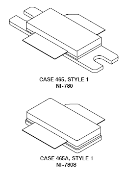
See product image

Product Details

Features

  • Typical Single–Carrier W–CDMA Performance: VDD = 28 Volts, IDQ = 1100 mA, Pout = 33 Watts Avg., Full Frequency Band, 3GPP Test Model 1, 64 DPCH with 50% Clipping, Channel Bandwidth = 3.84 MHz, Input Signal PAR = 7.5 dB @ 0.01% Probability on CCDF.
    Power Gain: 17.3 dB
    Drain Efficiency: 32.5%
    Device Output Signal PAR:  6.1 dB @ 0.01% Probability on CCDF
    ACPR @ 5 MHz Offset: –38 dBc in 3.84 MHz Channel Bandwidth
  • Capable of Handling 10:1 VSWR, @ 32 Vdc, 2140 MHz, 110 Watts CW Peak Tuned Output Power
  • Pout @ 1 dB Compression Point ≥ 110 Watts CW
  • 100% PAR Tested for Guaranteed Output Power Capability
  • Characterized with Series Equivalent Large–Signal Impedance Parameters
  • Internally Matched for Ease of Use
  • Integrated ESD Protection
  • Greater Negative Gate-Source Voltage Range for Improved Class C Operation
  • Designed for Digital Predistortion Error Correction Systems
  • RoHS Compliant
  • In Tape and Reel. R3 Suffix = 250 Units per 56 mm, 13 inch Reel

Documentation

Quick reference to our documentation types.

3 documents

Design Files

Quick reference to our design files types.

4 design files

Support

What do you need help with?