Product Longevity
Participating products are available for a minimum of 10 years. Designated participating products developed for the automotive, telecom and medical segments are available for a minimum of 15 years.
Sign in for a personalized NXP experience.
Roll over image to zoom in


This is a modal window.
Beginning of dialog window. Escape will cancel and close the window.
End of dialog window.
This is a modal window. This modal can be closed by pressing the Escape key or activating the close button.
This is a modal window. This modal can be closed by pressing the Escape key or activating the close button.
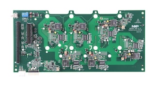
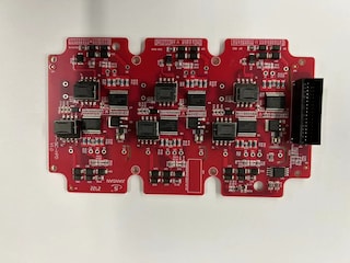
The GD3162 is an advanced, galvanically-isolated, single-channel gate driver designed to drive the latest SiC and IGBT modules for xEV traction inverters.
The GD3162 offers an adjustable dynamic gate strength drive via a programmable interface over SPI. In addition, advanced programmable protection features are autonomously managed as faults and the status of the power device and gate driver are reported via the interrupt pins.
The GD3162 is designed for high-functional safety integrity level systems (ASIL C/D) and meets the stringent requirements of automotive applications, being fully AEC-Q100 grade 1 qualified.

Participating products are available for a minimum of 10 years. Designated participating products developed for the automotive, telecom and medical segments are available for a minimum of 15 years.

S32K39/37/36 Microcontrollers for Electrification Applications

Advanced High Voltage Isolated Gate Driver with Segmented Drive for SiC MOSFETs
2 results
Include 0 NRND
Part | Order | CAD Model | Status | Device Function | Logic Level (V) | Package Type | Package Termination Count | Budgetary Price excluding tax | Frequency (Max) (kHz) | Load Current (IL) [TYP] (A) | Number of Channels | Protection | Drain-to-Source On Resistance (Typ) (mOhm) (RDS(ON)) | Load Supply Voltage (Min) (V) | Load Supply Voltage (Max) (V) | Supply Voltage [min] (V) | Supply Voltage [max] (V) | SPI [bits] | Ambient Operating Temperature (Min to Max) (℃) | ASIL Certification |
|---|---|---|---|---|---|---|---|---|---|---|---|---|---|---|---|---|---|---|---|---|
Active | Advanced HV GDIC with dynamic gate strength, RDSonM, VT Detection | 5 | SSOP32 | 32 | 1K @ US$4.83 | 100 | 10, 20, 30 | 1 | desaturation, overtemperature, real time monitor, segmented drive, short-circuit, two-level turn off, undervoltage | 500 | -12 | 25 | 4.75 | 6 | 24 | -40 to 125 | up to ASIL D | |||
Active | Adjustable dynamic gate strength, Advanced HV GDIC with Bus discharge, RDSonM, VT Detection | 5 | SSOP32 | 32 | 1K @ US$5.27 | 100 | 10, 20, 30 | 1 | desaturation, overtemperature, real time monitor, segmented drive, short-circuit, two-level turn off, undervoltage | 500 | -12 | 25 | 4.75 | 6 | 24 | -40 to 125 | up to ASIL D |
GD3162Quick reference to our documentation types.
6 documents
Compact List
There are no results for this selection.
Sign in to access authorized secure files. Learn more about secure access rights.
Please wait while your secure files are loading.
6 documents
Compact List
Sign in to access authorized secure files. Learn more about secure access rights.
Please wait while your secure files are loading.
1-5 of 7 hardware offerings


Additional hardware available. View our featured partner solutions.


Sign in to access authorized secure files. Learn more about secure access rights.
3 hardware offerings


To find additional partner offerings that support this product, visit our Partner Marketplace.
1-5 of 7 hardware offerings


Additional hardware available. View our featured partner solutions.


Quick reference to our software types.
3 software files
Note: For better experience, software downloads are recommended on desktop.
Sign in to access authorized secure files. Learn more about secure access rights.
Please wait while your secure files are loading.
3 software files
Note: For better experience, software downloads are recommended on desktop.
4 trainings
4 trainings
There are no recently viewed products to display.
View or edit your browsing history
Help us improve your experience on our site. We invite you to take our five-question survey.