
Product Longevity
Participating products are available for a minimum of 10 years. Designated participating products developed for the automotive, telecom and medical segments are available for a minimum of 15 years.
The TJA1021 is the interface between the local interconnect network (LIN) leader/follower protocol controller and the physical bus in a LIN. It is primarily intended for in-vehicle sub-networks using baud rates from 1 kBd up to 20 kBd and is and is compliant with LIN 2.0, LIN 2.1, LIN 2.2, LIN 2.2A, SAE J2602 and ISO 17987-4:2016 (12 V). The TJA1021 is pin-to-pin compatible with the TJA1020 and MC33662(B).
The transmit data stream of the protocol controller at the transmit data input (TXD) is converted by the TJA1021 into a bus signal with optimized slew rate and wave shaping to minimize electromagnetic emission (EME). The LIN bus output pin is pulled HIGH via an internal termination resistor. For a commander application, an external resistor in series with a diode should be connected between pin INH or pin VBAT and pin LIN. The receiver detects the data stream at the LIN bus input pin and transfers it via pin RXD to the microcontroller. In Sleep mode, the power consumption of the TJA1021 is very low. In failure modes, the power consumption is reduced to a minimum.

Participating products are available for a minimum of 10 years. Designated participating products developed for the automotive, telecom and medical segments are available for a minimum of 15 years.
| | | | | |
|---|---|---|---|---|---|
| | | | | |
| | | | | |
| | | | | |
| | | | | |
| | | | | |
| | | | | |
| | | | | |
| | | | | |
| | | | | |
| | | | | |
TJA1021Quick reference to our documentation types.
9 documents
Compact List
There are no results for this selection.
Sign in to access authorized secure files. Learn more about secure access rights.
Please wait while your secure files are loading.
9 documents
Compact List

Receive the full breakdown. See the product footprint and more in the eCad file.
1-5 of 10 hardware offerings
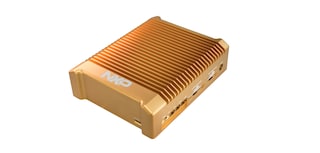
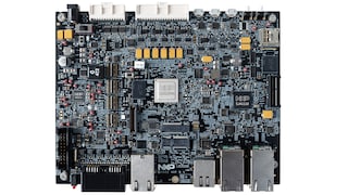
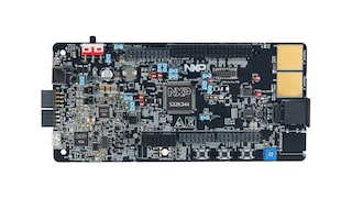
Additional hardware available. View our featured partner solutions.
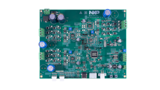
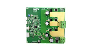
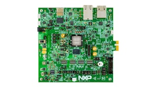
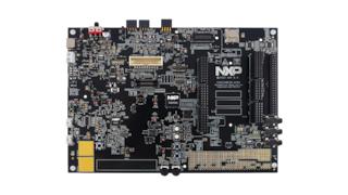
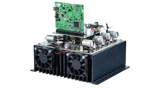
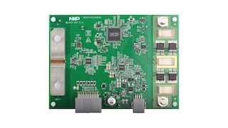
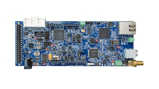
Sign in to access authorized secure files. Learn more about secure access rights.
1 hardware offering

To find additional partner offerings that support this product, visit our Partner Marketplace.
1-5 of 10 hardware offerings


Additional hardware available. View our featured partner solutions.


Quick reference to our software types.
Sign in to access authorized secure files. Learn more about secure access rights.
Please wait while your secure files are loading.
2 engineering services


There are no results for this selection.
There are no results for this selection.
To find additional partner offerings that support this product, visit our Partner Marketplace.
There are no recently viewed products to display.
View or edit your browsing history
Help us improve your experience on our site. We invite you to take our five-question survey.