
Flexis 32-Bit ColdFire® V1 Microcontroller
Sign in for a personalized NXP experience.
The S08QE family, comprised of a pin-compatible 8-bit and 32-bit device duo, is Our first family in the Flexis series. The Flexis series of controllers is the connection point of the NXP® Controller Continuum where 8- and 32-bit compatibility become reality.
The S08QE128 pushes the boundaries of the 8-bit architecture performance with 128 KB of flash, 24 analog-to-digital converter (ADC) channels and delivering up 25 MHz in bus frequency. The 32-bit MCF51QE128 is pin-, peripheral- and tool-compatible with the 8-bit S08QE128 device. They share a common set of peripherals and development tools, delivering the ultimate in migration flexibility.

Note: To see the product features close this window.
1-10 of 30 results
Include 2 NRND
Part | Order | CAD Model | Status | Package Type | Package Termination Count | Budgetary Price excluding tax | Core Type |
|---|---|---|---|---|---|---|---|
Active | HVQFN48 | 48 | 10K @ US$4.24 | S08 | |||
Active | LQFP44 | 44 | 10K @ US$4.28 | S08 | |||
Active | LQFP64 | 64 | 10K @ US$4.46 | S08 | |||
Active | LQFP80 | 80 | 10K @ US$4.70 | S08 | |||
Active | HVQFN32 | 32 | 10K @ US$2.56 | S08 | |||
Active | HVQFN48 | 48 | 10K @ US$2.60 | S08 | |||
Active | LQFP32 | 32 | 10K @ US$2.27 | S08 | |||
Active | LQFP44 | 44 | 10K @ US$2.63 | S08 | |||
Active | SO28 | 28 | 10K @ US$2.44 | S08 | |||
Active | HVQFN32 | 32 | 10K @ US$2.75 | S08 |
S08QEQuick reference to our documentation types.
1-10 of 84 documents
Compact List
Please wait while your secure files are loading.
1-10 of 84 documents
Compact List

Receive the full breakdown. See the product footprint and more in the eCad file.
5 hardware offerings
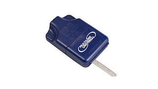
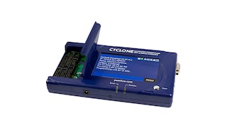
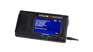
Additional hardware available. View our featured partner solutions.
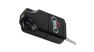
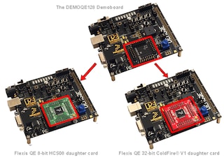
4 hardware offerings
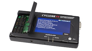
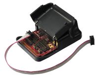
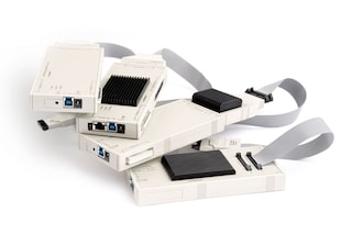
To find additional partner offerings that support this product, visit our Partner Marketplace.
5 hardware offerings


Additional hardware available. View our featured partner solutions.


Quick reference to our software types.
1-5 of 13 software files
Additional software available. View our featured partner solutions.
Note: For better experience, software downloads are recommended on desktop.
Please wait while your secure files are loading.
3 software offerings
To find additional partner offerings that support this product, visit our Partner Marketplace.
1-5 of 13 software files
Additional software available. View our featured partner solutions.
Note: For better experience, software downloads are recommended on desktop.
2 engineering services
.svg)

There are no results for this selection.
To find additional partner offerings that support this product, visit our Partner Marketplace.

Help us improve your experience on our site. We invite you to take our five-question survey.