
8-bit LCD for Battery-Powered and Handheld LC MCUs
Sign in for a personalized NXP experience.
The S08LL 8-bit segment LCD microcontroller family is ideal for battery-powered applications such as medical diagnostics or handheld appliances. The S08LL family extends battery life with comprehensive low-power technology, speeds development time and eliminates excess cost with its complete tower ecosystem.
Test for QC preview?
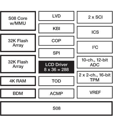
Note: To see the product features close this window.
| | | | | |
|---|---|---|---|---|---|
| | | | | |
| | | | | |
| | | | | |
| | | | | |
| | | | | |
| | | | | |
| | | | | |
| | | | | |
| | | | | |
| | | | | |
S08LLQuick reference to our documentation types.
1-10 of 41 documents
Compact List
There are no results for this selection.
Please wait while your secure files are loading.
1-10 of 41 documents
Compact List
2 design files
Please wait while your secure files are loading.
2 design files
1-5 of 6 hardware offerings
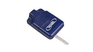
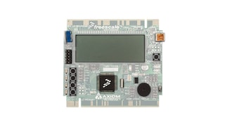
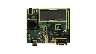
Additional hardware available. View our featured partner solutions.
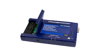
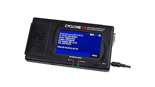
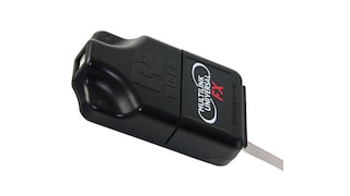
1 hardware offering
To find additional partner offerings that support this product, visit our Partner Marketplace.
1-5 of 6 hardware offerings


Additional hardware available. View our featured partner solutions.


Quick reference to our software types.
1-5 of 10 software files
Additional software available. View our featured partner solutions.
Note: For better experience, software downloads are recommended on desktop.
Please wait while your secure files are loading.
3 software offerings
To find additional partner offerings that support this product, visit our Partner Marketplace.
1-5 of 10 software files
Additional software available. View our featured partner solutions.
Note: For better experience, software downloads are recommended on desktop.
2 engineering services
.svg)

There are no results for this selection.
There are no results for this selection.
To find additional partner offerings that support this product, visit our Partner Marketplace.
There are no recently viewed products to display.
View or edit your browsing history
Help us improve your experience on our site. We invite you to take our five-question survey.