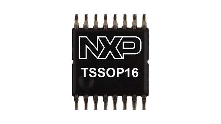
8-Bit I2C-Bus and SMBus I/O Port with 2-Kbit EEPROM
The PCA9500 is an 8-bit I/O expander with an on-board 2-kbit EEPROM.
The I/O expander's eight quasi-bidirectional data pins can be independently assigned as inputs or outputs to monitor board level status or activate indicator devices such as LEDs. The system leader writes to the I/O configuration bits in the same way as for the PCF8574. The data for each input or output is kept in the corresponding Input or Output register. The system leader can read all registers.
The EEPROM can be used to store error codes or board manufacturing data for read-back by application software for diagnostic purposes and is included in the I/O expander package.
The PCA9500 has 3 address pins with internal pull-up resistors allowing up to 8 devices to share the common two-wire I²C software protocol serial data bus. The fixed GPIO I²C-bus address is the same as the PCF8574 and the fixed EEPROM I²C-bus address is the same as the PCF8582C-2, so the PCA9500 appears as two separate devices to the bus leader.
The PCA9500 supports hot insertion to facilitate usage in removable cards on backplane systems.
The PCA9501 is an alternative to the functionally similar PCA9500 for systems where a higher number of devices are required to share the same I²C-bus or an interrupt output is required.
Product Details
Block Diagram
Choose a diagram:
Features
Key Features
- 8 general purpose input/output expander/collector
- Drop-in replacement for PCF8574 with integrated 2-kbit EEPROM
- Internal 256 x 8 EEPROM
- Self timed write cycle
- 4 byte page write operation
- I²C-bus and SMBus interface logic
- Internal power-on reset
- Noise filter on SCL/SDA inputs
- 3 address pins allowing up to 8 devices on the I²C-bus/SMBus
- No glitch on power-up
- Supports hot insertion
- Power-up with all channels configured as inputs
- Low standby current
- Operating power supply voltage range of 2.5 V to 3.6 V
- 5 V tolerant inputs/outputs
- 0 Hz to 400 kHz clock frequency
- ESD protection exceeds 2000 V HBM per JESD22-A114, 200 V MM per JESD22-A115 and 1000 V CDM per JESD22-C101
- Latch-up testing is done to JEDEC Standard JESD78 which exceeds 100 mA
- Packages offered: SO16, TSSOP16, HVQFN16
Buy/Parametrics
| | | | | |
|---|---|---|---|---|---|
| | | | | |
| | | | | |
| | | | | |
| | | | | |
| | | | | |
| | | | | |
| | | | | |
| | | | | |
| | | | | |
| | | | | |
1-10 of 16 documents
Compact List
Application Note (3)
Data Sheet (1)
Package Information (3)
Packing Information (4)
Supporting Information (1)
-
Footprint for reflow soldering[SO-SOJ-REFLOW]
Training Presentation (1)
-
DesignCon 2003 TecForum I²C-Bus Overview[DESIGN_CON_2003_TECFORUM_I2C_B_1]
User Guide (3)
Design Resources
Engineering Services
To get further assistance directly from NXP, please see our Engineering Services.
1 engineering service
-
Independent Design House (IDH)
Embedded Software Design
To find additional partner offerings that support this product, visit our Partner Marketplace.
Support
Recently viewed products
There are no recently viewed products to display.


