
Design Files
Quick reference to our
design files types.
2 design files
-
Models
nx3l2267 IBIS model
-
Models
nx3l2267_gu IBIS model
The NX3L2267 is a dual low-ohmic single-pole double-throw analog switch suitable for use as an analog or digital 2:1 multiplexer/demultiplexer. Each switch has a digital select input (nS), two independent inputs/outputs (nY0 and nY1) and a common input/output (nZ).
Schmitt trigger action at the digital inputs makes the circuit tolerant to slower input rise and fall times. Low threshold digital inputs allows this device to be driven by 1.8 V logic levels in 3.3 V applications without significant increase in supply current ICC. This makes it possible for the NX3L2267 to switch 4.3 V signals with a 1.8 V digital controller, eliminating the need for logic level translation. The NX3L2267 allows signals with amplitude up to VCC to be transmitted from nZ to nY0 or nY1, or from nY0 or nY1 to nZ. Its low ON resistance (0.5 Ω) and flatness (0.13 Ω) ensures minimal attenuation and distortion of transmitted signals.
| | | | | |
|---|---|---|---|---|---|
| | | | | |
| | | | | |
| | | | | |
| | | | | |
| | | | | |
| | | | | |
| | | | | |
| | | | | |
| | | | | |
| | | | | |
Quick reference to our documentation types.
5 documents
Compact List
5 documents
Compact List
2 design files
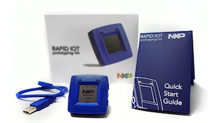
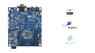
2 hardware offerings
To get further assistance directly from NXP, please see our Engineering Services.
2 engineering services

To find additional partner offerings that support this product, visit our Partner Marketplace.
There are no recently viewed products to display.