Features
Battery Cell Controller, Advanced, 6 Channels, TPL, LQFP48.
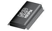
Package
HLQFP48 LQFP64, plastic, low profile quad flat package; 64 terminals; 0.5 mm pitch; 10 mm x 10 mm x 1.4 mm body.
Battery Cell Controller, Advanced, 6 Channels, TPL, LQFP48.
HLQFP48 LQFP64, plastic, low profile quad flat package; 64 terminals; 0.5 mm pitch; 10 mm x 10 mm x 1.4 mm body.
12NC: 935333193574
Details
12NC: 935333193518
Details
| Parameter | Value |
|---|---|
Supply Voltage [Min to Max] (V) | 5.5 to 28 |
Ambient Operating Temperature (Min to Max) (℃) | -40 to 125 |
Device Function | comm transceivers, linear regulators, system basis chip |
Data Rate [max] kbps | 1000.0 |
| Parameter | Value |
|---|---|
Protection | overtemperature, overvoltage protect, undervoltage |
Additional Features - Security | SPI |
Diagnostics | SPI |
| Part/12NC | PbFree | EU RoHS | Halogen Free | RHF Indicator | 2nd Level Interconnect | REACH SVHC | Weight (mg) |
|---|---|---|---|---|---|---|---|
MCZ33905DD5EK(935333193574) | Yes | Yes Certificate Of Analysis (CoA) | Yes | e3 | REACH SVHC | 765.05 | |
MCZ33905DD5EKR2(935333193518) | Yes | Yes Certificate Of Analysis (CoA) | Yes | e3 | REACH SVHC | 765.05 |
| Part/12NC | Safe Assure Functional Safety | Moisture Sensitivity Level (MSL) | Peak Package Body Temperature (PPT) (C°) | Maximum Time at Peak Temperatures (s) | |||
|---|---|---|---|---|---|---|---|
| Lead Free Soldering | Lead Free Soldering | Lead Free Soldering | |||||
MCZ33905DD5EK (935333193574) | No | 3 | 260 | 40 | |||
MCZ33905DD5EKR2 (935333193518) | No | 3 | 260 | 40 | |||
| Part/12NC | Harmonized Tariff (US)Disclaimer | Export Control Classification Number (US) |
|---|---|---|
MCZ33905DD5EK (935333193574) | 854239 | EAR99 |
MCZ33905DD5EKR2 (935333193518) | 854239 | EAR99 |
| Part/12NC | Issue Date | Effective Date | PCN | Title |
|---|---|---|---|---|
MCZ33905DD5EK (935333193574) | 2025-04-16 | 2025-05-26 | 202504007I | Freescale Logo to NXP Logo Product Marking Conversion for All Remaining Former Freescale Products |
MCZ33905DD5EKR2 (935333193518) | ||||
MCZ33905DD5EK (935333193574) | 2020-12-15 | 2020-12-16 | 202011011I | NXP Will Add a Sealed Date to the Product Label |
MCZ33905DD5EKR2 (935333193518) | ||||
MCZ33905DD5EK (935333193574) | 2017-12-20 | 2018-01-03 | 201710023I | New PQ Label Input for Non-MPQ Shipments |
MCZ33905DD5EKR2 (935333193518) |
The NXP MC33905 is part of a second generation family of system basis chips, combining multiple features and enhanced module design.