Application Note (26)
-
A Miner's Lamp Using MC9S08QG4[AN3601]
Sign in for a personalized NXP experience.
The S08QG Family of microcontrollers provide a wide variety of serial interfaces and peripherals, normally found in higher-end devices, all in a small package. Featuring low-power S08 8-bit architecture, S08QG devices are a good fit for battery-powered devices.

Note: To see the product features close this window.
| | | | | |
|---|---|---|---|---|---|
| | | | | |
| | | | | |
| | | | | |
| | | | | |
| | | | | |
| | | | | |
| | | | | |
| | | | | |
| | | | | |
| | | | | |
S08QGQuick reference to our documentation types.
1-10 of 60 documents
Compact List
There are no results for this selection.
Please wait while your secure files are loading.
1-10 of 60 documents
Compact List
1 design file
Please wait while your secure files are loading.
1 design file
1-5 of 6 hardware offerings
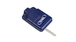

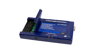
Additional hardware available. View our featured partner solutions.
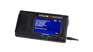
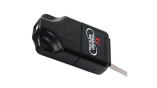

1 hardware offering
To find additional partner offerings that support this product, visit our Partner Marketplace.
1-5 of 6 hardware offerings


Additional hardware available. View our featured partner solutions.


Quick reference to our software types.
1-5 of 14 software files
Additional software available. View our featured partner solutions.
Note: For better experience, software downloads are recommended on desktop.
Please wait while your secure files are loading.
3 software offerings
To find additional partner offerings that support this product, visit our Partner Marketplace.
1-5 of 14 software files
Additional software available. View our featured partner solutions.
Note: For better experience, software downloads are recommended on desktop.
2 engineering services
.svg)

There are no results for this selection.
There are no results for this selection.
To find additional partner offerings that support this product, visit our Partner Marketplace.
There are no recently viewed products to display.
View or edit your browsing history
Help us improve your experience on our site. We invite you to take our five-question survey.