Application Note (16)
-
I2C non-blocking communication[AN4803]
Sign in for a personalized NXP experience.
NXP® 56F836X and 56F816X digital signal controllers belong to the 56800E core-based DSC family. They combine digital signal processing and microcontroller functionalities on a single chip, with a flexible set of peripherals.
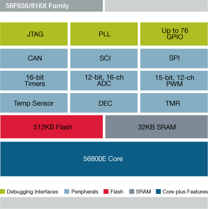
Note: To see the product features close this window.
| | | | | |
|---|---|---|---|---|---|
| | | | | |
| | | | | |
| | | | | |
| | | | | |
| | | | | |
| | | | | |
| | | | | |
| | | | | |
| | | | | |
| | | | | |
Quick reference to our documentation types.
1-10 of 70 documents
Compact List
There are no results for this selection.
Please wait while your secure files are loading.
1-10 of 70 documents
Compact List

Receive the full breakdown. See the product footprint and more in the eCad file.
1-5 of 7 hardware offerings
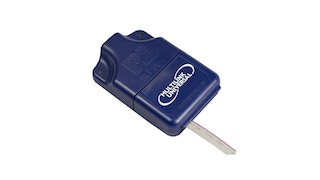

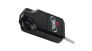
Additional hardware available. View our featured partner solutions.
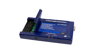
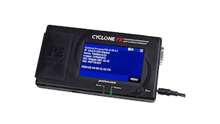


1 hardware offering
To find additional partner offerings that support this product, visit our Partner Marketplace.
1-5 of 7 hardware offerings


Additional hardware available. View our featured partner solutions.


Quick reference to our software types.
1-5 of 21 software files
Additional software available. View our featured partner solutions.
Note: For better experience, software downloads are recommended on desktop.
Please wait while your secure files are loading.
1 software offerings
To find additional partner offerings that support this product, visit our Partner Marketplace.
1-5 of 21 software files
Additional software available. View our featured partner solutions.
Note: For better experience, software downloads are recommended on desktop.
There are no recently viewed products to display.

Help us improve your experience on our site. We invite you to take our five-question survey.