
Product Longevity
Participating products are available for a minimum of 10 years. Designated participating products developed for the automotive, telecom and medical segments are available for a minimum of 15 years.
The NTSX2102 is a 2-bit, dual supply translating transceiver with auto direction sensing, that enables bidirectional voltage level translation. It features two 2-bit input-output ports (An and Bn), one output enable input (OE) and two supply pins (VCC(A) and VCC(B)). Both supplies can be supplied at any voltage between 1.65 V and 5.5 V. This flexibility makes the device suitable for translating between any of the voltage nodes (1.8 V, 2.5 V, 3.3 V and 5.0 V). Pins An and OE are referenced to VCC(A) and pins Bn are referenced to VCC(B). A LOW level at pin OE causes the outputs to assume a high-impedance OFF-state. This device is fully specified for partial power-down applications using IOFF. The IOFF circuitry disables the output, preventing the damaging backflow current through the device when it is powered down.
Participating products are available for a minimum of 10 years. Designated participating products developed for the automotive, telecom and medical segments are available for a minimum of 15 years.
| | | | | |
|---|---|---|---|---|---|
| | | | | |
| | | | | |
| | | | | |
| | | | | |
| | | | | |
| | | | | |
| | | | | |
| | | | | |
| | | | | |
| | | | | |
Quick reference to our documentation types.
6 documents
Compact List
6 documents
Compact List
2 design files
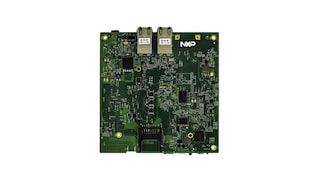
1 hardware offering
To get further assistance directly from NXP, please see our Engineering Services.
2 engineering services

To find additional partner offerings that support this product, visit our Partner Marketplace.
There are no recently viewed products to display.