
LPC551x/S1x: Baseline Arm® Cortex®-M33-Based Microcontroller Family
Sign in for a personalized NXP experience.
The baseline LPC550x/S0x MCU family, with it’s lower cost options and smaller footprint, further expand the existing general-purpose LPC5500 MCU series. It's advanced security and safety integration offer applications an extra level of protection.
Offering excellent ecosystem advantages for developers, including pin-, software- and peripheral-compatibility in addition to a comprehensive portfolio of software and tools, the LPC550x/S0x MCU family helps accelerate time to market.
This family of MCUs is part of the EdgeVerse™ edge computing platform and inclusive of the LPC55S06, LPC55S04, LPC5506 and LPC5504 MCUs.

LPC551x/S1x: Baseline Arm® Cortex®-M33-Based Microcontroller Family

High Efficiency Arm® Cortex®-M33-Based Microcontroller Family
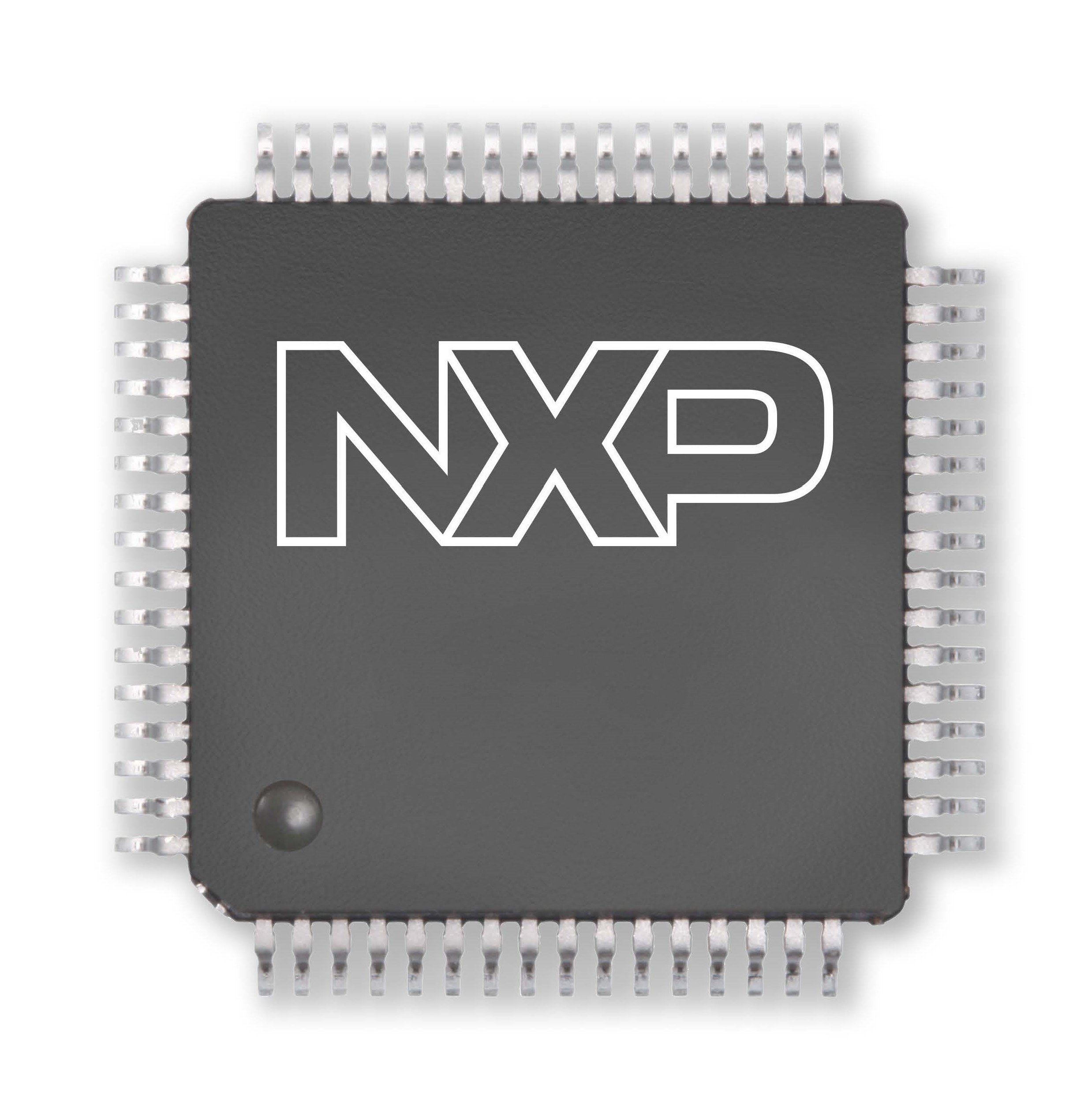
LPC552x/S2x: Mainstream Arm® Cortex®-M33-based Microcontroller Family

MCX A13x, 14x, 15x MCUs with Arm® Cortex® M33, Scalable Device Options, Low Power and Intelligent Peripherals
10 results
Include 0 NRND
Part | Order | CAD Model | Core Type | Operating Frequency [Max] (MHz) | Flash (kB) | GPIO | Security | ADC [Number, bits] | Ambient Operating Temperature (Min to Max) (℃) | Supply Voltage [Min to Max] (V) | Package Type | Status |
|---|---|---|---|---|---|---|---|---|---|---|---|---|
Arm Cortex-M33 | 96 | 64 | 45 | RNG | 2 x 16 | -40 to 105 | 1.8 to 3.6 | HTQFP64 | Active | |||
Arm Cortex-M33 | 96 | 64 | 30 | RNG | 2 x 16 | -40 to 105 | 1.8 to 3.6 | HVQFN48 | Active | |||
Arm Cortex-M33 | 96 | 128 | 45 | RNG | 2 x 16 | -40 to 105 | 1.8 to 3.6 | HTQFP64 | Active | |||
Arm Cortex-M33 | 96 | 128 | 30 | RNG | 2 x 16 | -40 to 105 | 1.8 to 3.6 | HVQFN48 | Active | |||
Arm Cortex-M33 | 96 | 256 | 45 | RNG | 2 x 16 | -40 to 105 | 1.8 to 3.6 | HTQFP64 | Active | |||
Arm Cortex-M33 | 96 | 256 | 30 | RNG | 2 x 16 | -40 to 105 | 1.8 to 3.6 | HVQFN48 | Active | |||
Arm Cortex-M33 | 96 | 128 | 45 | AES-D, CRC, RNG, SD, UUID | 2 x 16 | -40 to 105 | 1.8 to 3.6 | HTQFP64 | Active | |||
Arm Cortex-M33 | 96 | 128 | 30 | AES-D, CRC, RNG, SD, UUID | 2 x 16 | -40 to 105 | 1.8 to 3.6 | HVQFN48 | Active | |||
Arm Cortex-M33 | 96 | 256 | 45 | AES-D, CRC, RNG, SD, UUID | 2 x 16 | -40 to 105 | 1.8 to 3.6 | HTQFP64 | Active | |||
Arm Cortex-M33 | 96 | 256 | 30 | AES-D, CRC, RNG, SD, UUID | 2 x 16 | -40 to 105 | 1.8 to 3.6 | HVQFN48 | Active |
Quick reference to our documentation types.
1-10 of 25 documents
Compact List
There are no results for this selection.
Sign in to access authorized secure files. Learn more about secure access rights.
Please wait while your secure files are loading.
1-10 of 25 documents
Compact List
3 design files
Sign in to access authorized secure files. Learn more about secure access rights.
Please wait while your secure files are loading.
3 design files
1-5 of 8 hardware offerings
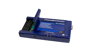
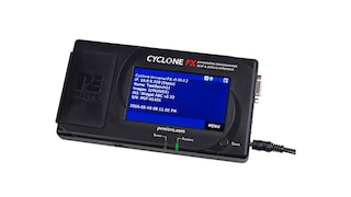
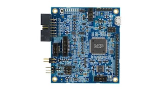
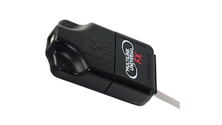
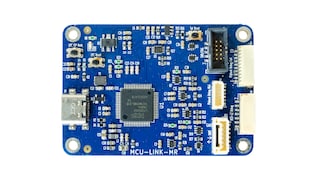
Sign in to access authorized secure files. Learn more about secure access rights.
1-5 of 8 hardware offerings


Quick reference to our software types.
1-5 of 13 software files
Additional software available. View our featured partner solutions.
Note: For better experience, software downloads are recommended on desktop.
Sign in to access authorized secure files. Learn more about secure access rights.
Please wait while your secure files are loading.
1-5 of 29 software offerings
To find additional partner offerings that support this product, visit our Partner Marketplace.
1-5 of 13 software files
Additional software available. View our featured partner solutions.
Note: For better experience, software downloads are recommended on desktop.
3 engineering services


There are no results for this selection.
There are no results for this selection.
To find additional partner offerings that support this product, visit our Partner Marketplace.
1-5 of 22 trainings
Additional trainings are available. View our featured partner trainings.
22 trainings
Additional trainings are available. View our featured partner trainings.
11 trainings
To find additional partner offerings that support this product, visit our Partner Marketplace.
There are no recently viewed products to display.

Help us improve your experience on our site. We invite you to take our five-question survey.