Features
Battery Cell Controller, Advanced, 6 Channels, TPL, LQFP48.
Package
HLQFP48 LQFP64, plastic, low profile quad flat package; 64 terminals; 0.5 mm pitch; 10 mm x 10 mm x 1.4 mm body.
Dual supply translating transceiver; open drain; auto direction sensing
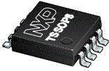
TSSOP: plastic, thin shrink small outline package; 8 leads; 0.65 mm pitch; 3 mm x 3 mm x 1.1 mm body
12NC: 935293487125
Details
Quantity
Unit Pricing
| 1 - 25 | $0.33 |
| 26 - 99 | $0.33 |
| 100+ | $0.33 |
Order
| Parameter | Value |
|---|---|
Signal Application | GPIO, I2C, SMBus, UART |
Type VLT | BiDirectional FET w/one shot |
Number of bits | 2 |
VCC(A) (Min - Max) | 1.65 to 3.6 |
VCC(B) (Min-Max) | 2.3 to 5.5 |
Supply Current (Typ) (μA) | 1.5 |
| Parameter | Value |
|---|---|
Bandwidth (Max) (MHz) | 50 |
Input Type (TTL, CMOS, Schmitt Trigger) | CMOS |
Output Type (Open Drain, 3-State, Push-Pull, Pass-gate) | 3-State, Pass-gate |
Ambient Operating Temperature (Min to Max) (℃) | -40 to 125 |
AEC-Q100 compliant | N |
| Part/12NC | PbFree | EU RoHS | Halogen Free | RHF Indicator | REACH SVHC | Weight (mg) |
|---|---|---|---|---|---|---|
NTS0102DP,125(935293487125) | Yes | Yes Certificate Of Analysis (CoA) | Yes | REACH SVHC | 18.4163456 |
| Part/12NC | Safe Assure Functional Safety | Moisture Sensitivity Level (MSL) | Peak Package Body Temperature (PPT) (C°) | ||
|---|---|---|---|---|---|
| Lead Soldering | Lead Free Soldering | Lead Soldering | Lead Free Soldering | ||
NTS0102DP,125 (935293487125) | No | 1 | 1 | 240 | 260 |
| Part/12NC | Harmonized Tariff (US)Disclaimer |
|---|---|
NTS0102DP,125 (935293487125) | 854239 |
| Part/12NC | Issue Date | Effective Date | PCN | Title |
|---|---|---|---|---|
NTS0102DP,125 (935293487125) | 2021-11-24 | 2022-03-04 | 202104052F02 | SOT505-2 Assembly Transfer from ATP to ATBK |
NTS0102DP,125 (935293487125) | 2021-05-06 | - | 202104052A | SOT505-2 Assembly Transfer from ATP to ATBK |
The NTS0102 is a 2-bit, dual supply translating transceiver with auto direction sensing, that enables bidirectional voltage level translation. It features two 2-bit input-output ports (An and Bn), one output enable input (OE) and two supply pins (VCC(A) and VCC(B)). VCC(A) can be supplied at any voltage between 1.65 V and 3.6 V and VCC(B) can be supplied at any voltage between 2.3 V and 5.5 V, making the device suitable for translating between any of the voltage nodes (1.8 V, 2.5 V, 3.3 V and 5.0 V). Pins An and OE are referenced to VCC(A) and pins Bn are referenced to VCC(B). A LOW level at pin OE causes the outputs to assume a high-impedance OFF-state. This device is fully specified for partial power-down applications using IOFF. The IOFF circuitry disables the output, preventing the damaging backflow current through the device when it is powered down.