Application Note (42)
-
Understanding SYSCLK Jitter[AN4056]
The PowerQUICC® III is a versatile one-chip integrated microprocessor and peripheral combination that can be used in a variety of controller applications, excelling particularly in communications and networking products. Our PowerQUICC III processor family is the next generation of integrated communications processors. The PowerQUICC III provides higher performance in all areas of device operation, including greater flexibility, extended capabilities, and higher integration.
Our leading PowerQUICC III architecture integrates two processing blocks. One block is a high-performance embedded e500 core. With 256 KB of level 2 cache, the e500 core is built on Power Architecture® technology and provides unprecedented levels of hardware and software debugging support. The second block is the communications processor module (CPM). The CPM of the PowerQUICC III can support three fast serial communications controllers (FCCs), two multichannel controllers (MCCs), four serial communications controllers (SCCs), one serial peripheral interface (SPI) and one I²C interface.
The PowerQUICC III also offers two integrated 10/100/1000 Ethernet controllers, a DDR SDRAM memory controller, a 64-bit PCI-X/PCI controller, and a RapidIO® interconnect. This high level of integration helps simplify board design and offers significant bandwidth and performance for high-end control-plane and data-plane applications.
Contact your local NXP Sales Office or NXP Authorized Distributor.
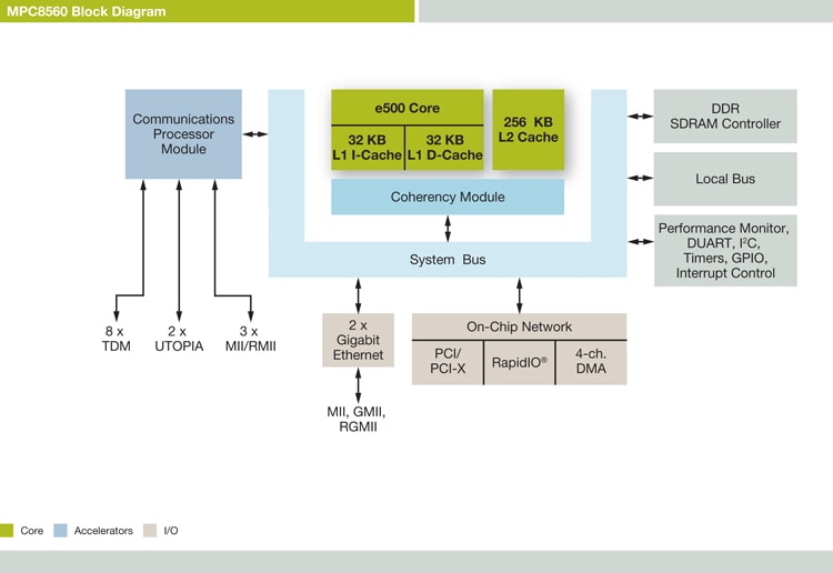
Note: To see the product features close this window.
| | | | | |
|---|---|---|---|---|---|
| | | | | |
| | | | | |
| | | | | |
| | | | | |
| | | | | |
| | | | | |
| | | | | |
| | | | | |
| | | | | |
| | | | | |
MPC8560Quick reference to our documentation types.
1-10 of 68 documents
Compact List
There are no results for this selection.
Please wait while your secure files are loading.
1-10 of 68 documents
Compact List
2 design files
Please wait while your secure files are loading.
2 design files
2 hardware offerings
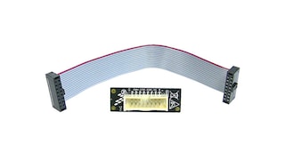
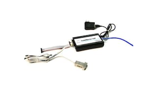
2 hardware offerings


Quick reference to our software types.
5 software files
Note: For better experience, software downloads are recommended on desktop.
Please wait while your secure files are loading.
5 software files
Note: For better experience, software downloads are recommended on desktop.
There are no recently viewed products to display.
View or edit your browsing history
Help us improve your experience on our site. We invite you to take our five-question survey.