Application Note (7)
Data Sheet (2)
-
PN5190B2 NFC Frontend[PN5190B2]
-
PN5190B1 NFC frontend[PN5190B1]
Sign in for a personalized NXP experience.
Please check the new online NFC Antenna Tool for tag and reader devices.
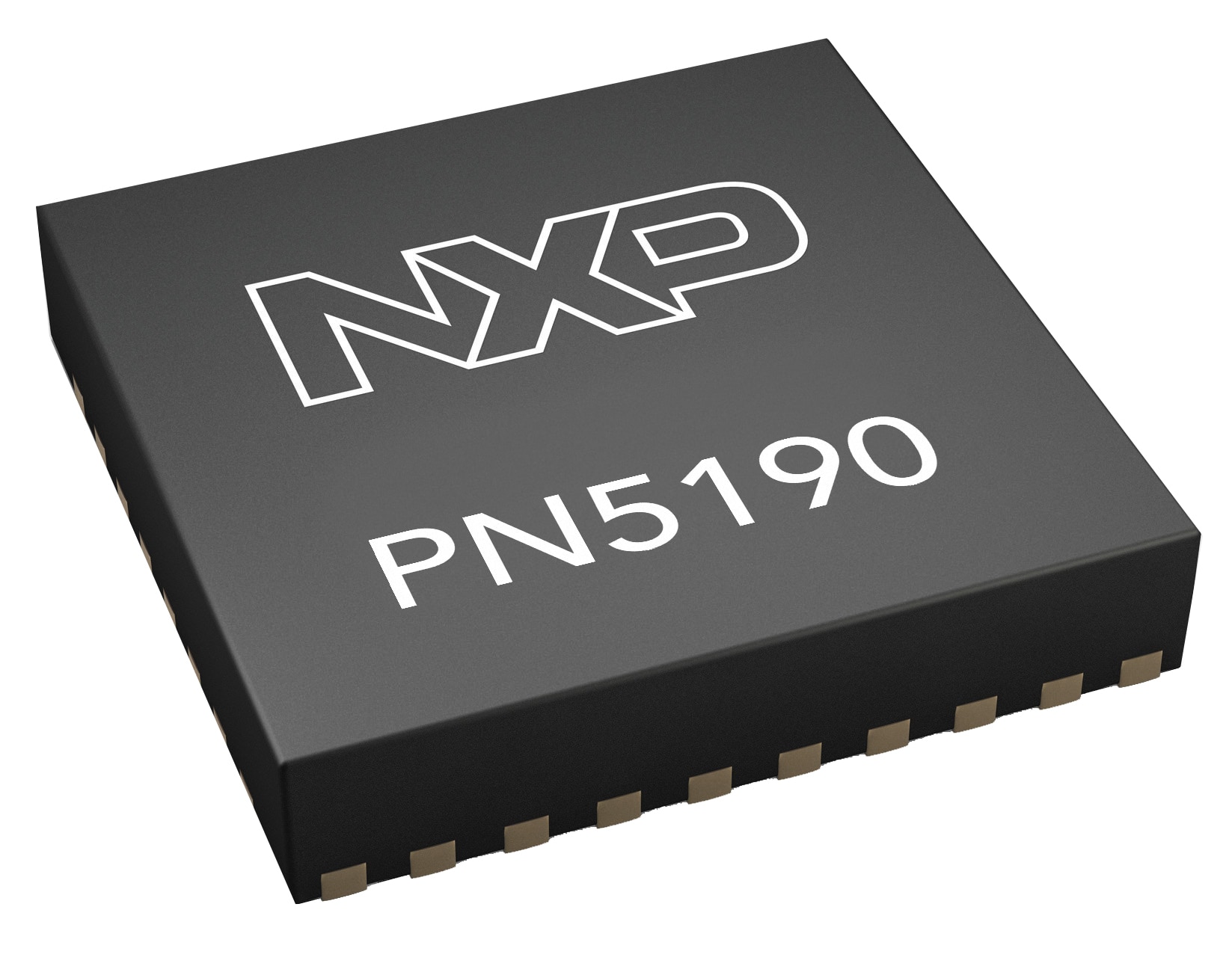
As a full NFC frontend with High RF output (2W) and High receiver sensitivity, the NXP PN5190 is a robust solution for payment terminals and all readers that need to generate a strong RF field in a difficult environment.
The PN5190 simplifies design while ensuring interoperability with a broad range of smartcards and mobile phones and allows to achieve EMVCo 3.1 analog and digital L1 compliancy.
The High output power and receiver sensitivity allow the design of small antennas maintaining the communication range of a larger antenna. This is especially interesting for designs with limited space for a large antenna. Efficient power-saving modes allow long battery lifetime for battery-powered systems, including residential access locks.

| PN5190 B1 | 2.0A and 2.FA | 2.09 and 2.F9 | 2.08 and 2.F8 | 2.07 and 2.F7 |
| PN5190 B2 | 3.05 and 3.F5 | 3.04 and 3.F4 | 3.03 and 3.F3 | 3.02 and 3.F2 |
| | | | | |
|---|---|---|---|---|---|
| | | | | |
| | | | | |
| | | | | |
| | | | | |
| | | | | |
| | | | | |
| | | | | |
| | | | | |
| | | | | |
| | | | | |
PN5190Quick reference to our documentation types.
15 of 15 documents
Compact List
There are no results for this selection.
Sign in to access authorized secure files. Learn more about secure access rights.
Please wait while your secure files are loading.
1-10 of 15 documents
Compact List
4 design files
Sign in to access authorized secure files. Learn more about secure access rights.
Please wait while your secure files are loading.
4 design files
3 hardware offerings


Sign in to access authorized secure files. Learn more about secure access rights.
3 hardware offerings


Quick reference to our software types.
1-5 of 20 software files
Note: For better experience, software downloads are recommended on desktop.
Sign in to access authorized secure files. Learn more about secure access rights.
Please wait while your secure files are loading.
1-5 of 20 software files
Note: For better experience, software downloads are recommended on desktop.
3 trainings
3 trainings
1 trainings
To find additional partner offerings that support this product, visit our Partner Marketplace.

Help us improve your experience on our site. We invite you to take our five-question survey.