
Kinetis® K24-120 MHz, Full-Speed USB, 256KB SRAM Microcontrollers (MCUs) based on Arm® Cortex®-M4 Core
Sign in for a personalized NXP experience.
Click over video to play
This is a modal window.
Beginning of dialog window. Escape will cancel and close the window.
End of dialog window.
This is a modal window. This modal can be closed by pressing the Escape key or activating the close button.
This is a modal window. This modal can be closed by pressing the Escape key or activating the close button.
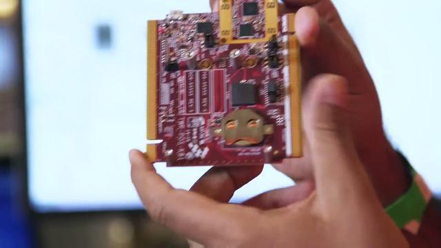
The Kinetis® K81 MCU extends the Kinetis MCU portfolio with advanced security capabilities including anti-tamper peripheral, boot ROM to support encrypted firmware updates, automatic decryption from external serial flash memory, AES acceleration, and hardware support for public key cryptography. The K81 MCU can be used to meet the security standards for point-of-sale (PoS) applications.
Please contact your local NXP representative to download the K81 Security Data sheet and Reference Manual documents (under NDA).

Note: To see the product features close this window.
2 results
Include 0 NRND
Part | Order | CAD Model | Status | Core Type | Operating Frequency [Max] (MHz) | SRAM (kB) | Flash (kB) | UART | SPI | I2C | USB Controllers | GPIO | ADC (16 bit) | 16-bit PWM | Security | Package Type | Package Termination Count | Package Dimensions (LxWxZ (mm)) | Package Pitch (mm) | Ambient Operating Temperature (Min to Max) (℃) |
|---|---|---|---|---|---|---|---|---|---|---|---|---|---|---|---|---|---|---|---|---|
Active | Arm Cortex-M4 | 150 | 256 | 256 | 5 | 3 | 4 | 1 | 85 | 1 | 24 | CRC | XFBGA121 | 121 | 8 x 8 x 0.43 | 0.65 | -40 to 105 | |||
Active | Arm Cortex-M4 | 150 | 256 | 256 | 5 | 3 | 4 | 1 | 66 | 1 | 24 | CRC | LQFP100 | 100 | 14 x 14 x 1.4 | 0.5 | -40 to 105 |
K81_150Quick reference to our documentation types.
1-10 of 11 documents
Compact List
There are no results for this selection.
Sign in to access authorized secure files. Learn more about secure access rights.
Please wait while your secure files are loading.
1-10 of 11 documents
Compact List
3 design files
Sign in to access authorized secure files. Learn more about secure access rights.
Please wait while your secure files are loading.
3 design files
1-5 of 13 hardware offerings
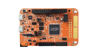

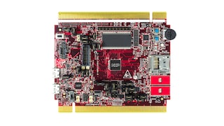
Additional hardware available. View our featured partner solutions.
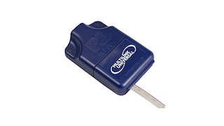
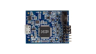
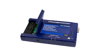
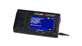
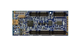
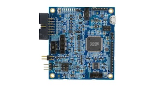

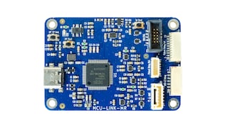

Sign in to access authorized secure files. Learn more about secure access rights.
1-5 of 6 hardware offerings
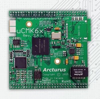


To find additional partner offerings that support this product, visit our Partner Marketplace.
1-5 of 13 hardware offerings


Additional hardware available. View our featured partner solutions.


Quick reference to our software types.
1-5 of 6 software files
Additional software available. View our featured partner solutions.
Note: For better experience, software downloads are recommended on desktop.
Sign in to access authorized secure files. Learn more about secure access rights.
Please wait while your secure files are loading.
1-5 of 37 software offerings
To find additional partner offerings that support this product, visit our Partner Marketplace.
1-5 of 6 software files
Additional software available. View our featured partner solutions.
Note: For better experience, software downloads are recommended on desktop.
1-5 of 7 engineering services

.svg)


There are no results for this selection.
There are no results for this selection.
To find additional partner offerings that support this product, visit our Partner Marketplace.
4 trainings
Additional trainings are available. View our featured partner trainings.
4 trainings
Additional trainings are available. View our featured partner trainings.
8 trainings
To find additional partner offerings that support this product, visit our Partner Marketplace.
There are no recently viewed products to display.
View or edit your browsing history
Help us improve your experience on our site. We invite you to take our five-question survey.