
Kinetis® K24-120 MHz, Full-Speed USB, 256KB SRAM Microcontrollers (MCUs) based on Arm® Cortex®-M4 Core
Sign in for a personalized NXP experience.
The Kinetis K27 USB Arm® Cortex®-M4 MCUs target applications requiring processing efficiency and extra-large embedded memory with 2 MB Flash and 1 MB SRAM. This sub-family is:
Input supply voltage: 1.71V to 3.6V + separate VBAT domain
Packages: 169 MAPBGA (9x9mm, 0.65mm pitch)
Evaluation / Development platform: FRDM-K28F
| Kinetis MCU sub-family |
Part # | Mask Set | Flash | SRAM | PMC | Packages | Development Board |
|---|---|---|---|---|---|---|---|
| K27 | MK27FN2M0AVMI15 | 3N96T (recommended) |
2MB | 1MB | No | 169 MABPGA | FRDM-K28F |
| MK27FN2M0VMI15 | 2N96T | ||||||
| K28 | MK28FN2M0ACAU15R | 3N96T (recommended) |
Yes | 210 WLCSP | |||
| MK28FN2M0AVMI15 | 169 MAPBGA | ||||||
| MK28FN2M0CAU15R | 2N96T | 210 WLCSP | |||||
| MK28FN2M0VMI15 | 169 MAPBGA |
| | | | | |
|---|---|---|---|---|---|
| | | | | |
| | | | | |
| | | | | |
| | | | | |
| | | | | |
| | | | | |
| | | | | |
| | | | | |
| | | | | |
| | | | | |
K27_150Quick reference to our documentation types.
1-10 of 59 documents
Compact List
There are no results for this selection.
Sign in to access authorized secure files. Learn more about secure access rights.
Please wait while your secure files are loading.
1-10 of 59 documents
Compact List
2 design files
Sign in to access authorized secure files. Learn more about secure access rights.
Please wait while your secure files are loading.
2 design files
1-5 of 10 hardware offerings
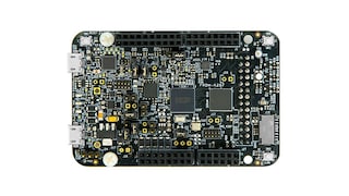
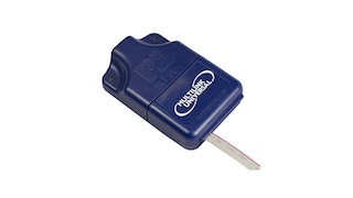
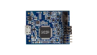
Additional hardware available. View our featured partner solutions.
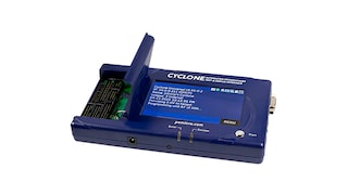
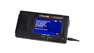
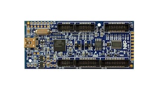
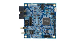
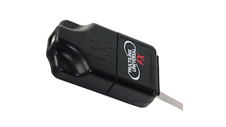

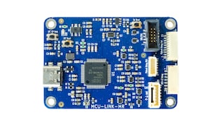
Sign in to access authorized secure files. Learn more about secure access rights.
5 hardware offerings
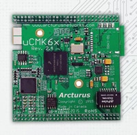


To find additional partner offerings that support this product, visit our Partner Marketplace.
1-5 of 10 hardware offerings


Additional hardware available. View our featured partner solutions.


Quick reference to our software types.
1-5 of 9 software files
Additional software available. View our featured partner solutions.
Note: For better experience, software downloads are recommended on desktop.
Sign in to access authorized secure files. Learn more about secure access rights.
Please wait while your secure files are loading.
1-5 of 39 software offerings
To find additional partner offerings that support this product, visit our Partner Marketplace.
1-5 of 9 software files
Additional software available. View our featured partner solutions.
Note: For better experience, software downloads are recommended on desktop.
1-5 of 8 engineering services

.svg)


There are no results for this selection.
There are no results for this selection.
To find additional partner offerings that support this product, visit our Partner Marketplace.
5 trainings
Additional trainings are available. View our featured partner trainings.
5 trainings
Additional trainings are available. View our featured partner trainings.
8 trainings
To find additional partner offerings that support this product, visit our Partner Marketplace.
Kinetis® K63-120 MHz, 256KB SRAM, Anti-Tamper Microcontrollers (MCUs) based on Arm® Cortex®-M4 Core
buy options

Help us improve your experience on our site. We invite you to take our five-question survey.