Features
Battery Cell Controller, Advanced, 6 Channels, TPL, LQFP48.
Package
HLQFP48 LQFP64, plastic, low profile quad flat package; 64 terminals; 0.5 mm pitch; 10 mm x 10 mm x 1.4 mm body.
Dual Supply Level Shifting Hot swappable I2C-bus and SMBus bus buffer
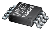
TSSOP8: plastic, thin shrink small outline package; 8 leads; 0.65 mm pitch; 3 mm x 3 mm x 1.1 mm body
12NC: 935279719118
Details
Quantity
Unit Pricing
| 1 - 24 | $1.31 |
| 25 - 25 | $1.31 |
| 26 - 99 | $1.31 |
| 100+ | $1.31 |
Order
| Parameter | Value |
|---|---|
Operating Temperature (°C) | -40~85 |
I2C-bus (kHz) | 400 |
Operating voltage (VDC) | 2.7~5.5 |
| Parameter | Value |
|---|---|
Operating Voltage (V) | 2.7~5.5 |
Inputs | 1 |
Outputs | 1 |
| Part/12NC | PbFree | EU RoHS | Halogen Free | RHF Indicator | REACH SVHC | Weight (mg) |
|---|---|---|---|---|---|---|
PCA9512ADP,118(935279719118) | Yes | Yes Certificate Of Analysis (CoA) | Yes | REACH SVHC | 24.0 |
| Part/12NC | Safe Assure Functional Safety | Moisture Sensitivity Level (MSL) | Peak Package Body Temperature (PPT) (C°) | FIT | MTBF | IR | ||
|---|---|---|---|---|---|---|---|---|
| Lead Soldering | Lead Free Soldering | Lead Soldering | Lead Free Soldering | |||||
PCA9512ADP,118 (935279719118) | No | 1 | 1 | 240 | 260 | 2.0 | 5.0E8 | 0.0 |
| Part/12NC | Harmonized Tariff (US)Disclaimer |
|---|---|
PCA9512ADP,118 (935279719118) | 854239 |
The PCA9512A/B is a hot swappable I²C-bus and SMBus buffer that allows I/O card insertion into a live backplane without corruption of the data and clock buses and includes two dedicated supply voltage pins to provide level shifting between 3.3 V and 5 V systems while maintaining a better noise margin for each voltage level. Either pin may be powered with supply voltages ranging from 2.7 V to 5.5 V with no constraints on which supply voltage is higher. Control circuitry prevents the backplane from being connected to the card until a stop bit or bus idle occurs on the backplane without bus contention on the card. When the connection is made, the PCA9512A/B provides bidirectional buffering, keeping the backplane and card capacitances isolated.
Both the PCA9512A and PCA9512B use identical silicon (PCN201012007F dated 13 Dec 2010), so the PCA9512B will be discontinued in the near future and is not recommended for new designs.
The PCA9512A/B rise time accelerator circuitry allows the use of weaker DC pull-up currents while still meeting rise time requirements. The PCA9512A/B incorporates a digital input pin that enables and disables the rise time accelerators on all four SDAn and SCLn pins.
During insertion, the PCA9512A/B SDAn and SCLn pins are precharged to 1 V to minimize the current required to charge the parasitic capacitance of the chip.
The incremental offset design of the PCA9510A/11A/12A/12B/13A/14A I/O drivers allows them to be connected to another PCA9510A/11A/12A/12B/13A/14A device in series or in parallel and to the I²C compliant side of static offset bus buffers, but not to the static offset side of those bus buffers.