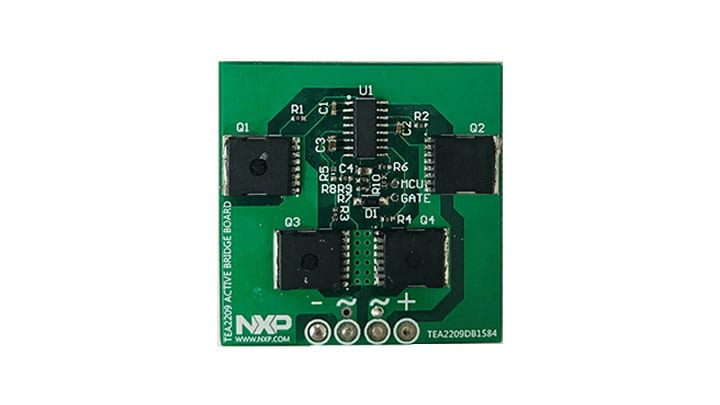
Getting Started with the TEA2209DB1584
Contents of this document
-
Out of the Box
-
Plug It In
-
Configure Hardware
Sign in to save your progress. Don't have an account? Create one.

Purchase your TEA2209T
1. Out of the Box
The NXP analog product development boards provide an easy-to-use platform for evaluating NXP products. The boards support a range of analog, mixed-signal and power solutions. They incorporate monolithic integrated circuits and system-in-package devices that use proven high-volume technology. NXP products offer longer battery life, a smaller form factor, reduced component counts, lower cost and improved performance in powering state-of-the-art systems.
This page will guide you through the process of setting up and using the TEA2209DB1584 demo board.
2. Plug It In
2.1 Board Features
- Elimination of forward conduction losses of the diode rectifier bridge
- Very low IC power consumption (2 mW)
- Integrated high-voltage level shifters
- Directly drives four rectifier MOSFETs
- Very low external part count
- Integrated X-capacitor discharge (2 mA)
- Self-supplying
- Full-wave drive improving total harmonic distortion (THD)
- Undervoltage lockout (UVLO) for high-side and low-side drivers
- Drain-source overvoltage protection for all external power MOSFETs
- Gate pull-down currents at start-up for all external power MOSFETs
- Disable function for all external power FETs
3. Configure Hardware
3.1 Configure the Hardware
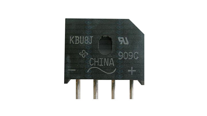
The TEA2209DB1584 demo board contains four 600 V/28 mΩ MOSFETs. It makes the board suitable for universal AC input and output power applications of several hundreds of Watts. The TEA2209DB1584 demo board contains four leads that can easily replace a traditional diode bridge. The outer two leads are connected to positive and negative rectified voltages. The inner two leads are connected to AC mains lines. These four leads are pin-to-pin with typical bridge rectifier diodes pins.
The following figure shows the difference between bridge diodes and active bridge configurations.
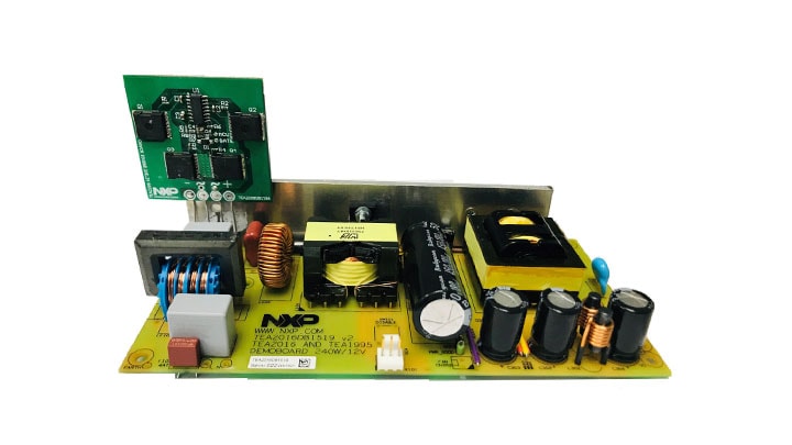
The following figure shows an example of the TEA2209DB1584 demo board mounted on an NXP Semiconductors TEA2016DB1519 demo board.