Application Note (13)
-
LPC540xx Image Header Structure[AN12122]
-
LPC540xx Crystal less USB solution[TN00033]
Sign in for a personalized NXP experience.
Click over video to play
This is a modal window.
Beginning of dialog window. Escape will cancel and close the window.
End of dialog window.
This is a modal window. This modal can be closed by pressing the Escape key or activating the close button.
This is a modal window. This modal can be closed by pressing the Escape key or activating the close button.

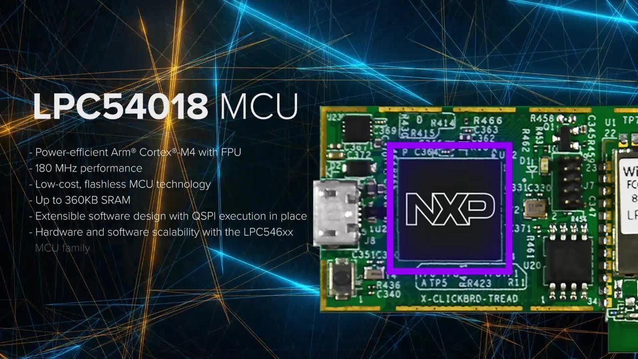
Offering flashless design and security integration, the LPC540xx family of MCUs combines a 180 MHz Arm® Cortex®-M4 core with a power-efficient and unique architecture, advanced HMI and flexible communication peripherals for real-time performance in the next-generation IoT. Featuring flexibility with a quad SPI flash interface, CAN, graphic LCD and up to 11 channels for FlexComm, the LPC540xx family provides the ability to adapt as requirements change. Compatibility within the LPC54000 series enables the LPC540xx MCU family to provide a seamless migration path for increasing processing power and adding the flexibility of additionally advanced peripherals.
For added security, the new LPC54S0xx MCU devices in this family provide Physical Unclonable Function (PUF) root key using dedicated SRAM for silicon fingerprint making it possible to generate, store, and reconstruct keys. In addition, the LPC54S0xx devices feature an on-chip hardware AES engine to protect the image content and accelerate processing for data integrity and proof of origin. Data can be encrypted or decrypted by the AES engine using the encrypted key stored in the OTP, SRAM PUF-based or a software supplied key.
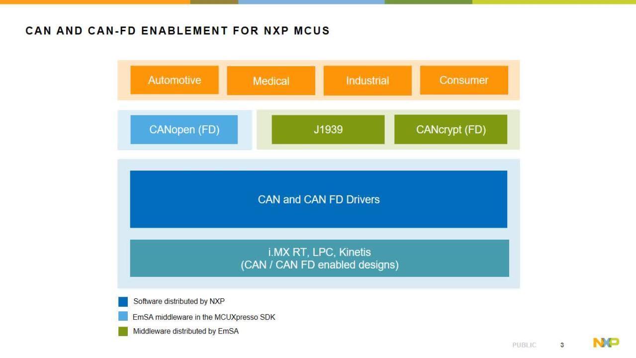
This device is fully supported by NXP’s MCUXpresso Software and Tools, a comprehensive and cohesive set of free software development tools for Kinetis, LPC and i.MX RT microcontrollers. MCUXpresso SDK also includes project files for Keil MDK and IAR EWARM.

Note: To see the product features close this window.
1-10 of 19 results
Include 0 NRND
Part | Order | CAD Model | Status | Core Type | Operating Frequency [Max] (MHz) | Flash (kB) | SRAM (kB) | EEPROM (kB) | CAN | USB Controllers | Security | GPIO | Supply Voltage [Min to Max] (V) | Ambient Operating Temperature (Min to Max) (℃) | Package Type |
|---|---|---|---|---|---|---|---|---|---|---|---|---|---|---|---|
Active | Arm Cortex-M4 | 180 | — | 360 | 0.02 | 2 | 2 | CRC, RNG | 64 | 1.71 to 3.6 | -40 to 105 | LQFP100 | |||
Active | Arm Cortex-M4 | 180 | — | 360 | 16 | — | 2 | RNG | 64 | 1.71 to 3.6 | -40 to 105 | TFBGA100 | |||
Active | Arm Cortex-M4 | 180 | — | 360 | 0.02 | 2 | 2 | CRC, RNG | 64 | 1.71 to 3.6 | -40 to 105 | LQFP100 | |||
Active | Arm Cortex-M4 | 180 | — | 360 | 0.02 | 2 | 2 | CRC, RNG | 171 | 1.71 to 3.6 | -40 to 105 | LQFP208 | |||
Active | Arm Cortex-M4 | 180 | — | 360 | 0.02 | 2 | 2 | CRC, RNG | 145 | 1.71 to 3.6 | -40 to 105 | TFBGA180 | |||
Active | Arm Cortex-M4 | 180 | 2048 | 360 | — | 2 | 2 | CRC, RNG | 137 | 1.71 to 3.6 | -40 to 105 | TFBGA180 | |||
Active | Arm Cortex-M4 | 180 | 4096 | 360 | — | 2 | 2 | CRC, RNG | 137 | 2.7 to 3.6 | -40 to 105 | TFBGA180 | |||
Active | Arm Cortex-M4 | 180 | — | 360 | 0.02 | 2 | 2 | CRC, RNG | 171 | 1.71 to 3.6 | -40 to 105 | LQFP208 | |||
Active | Arm Cortex-M4 | 180 | — | 360 | 0.02 | 2 | 2 | CRC, RNG | 145 | 1.71 to 3.6 | -40 to 105 | TFBGA180 | |||
Active | Arm Cortex-M4 | 180 | — | 360 | 0.02 | 2 | 2 | CRC, RNG | 64 | 1.71 to 3.6 | -40 to 105 | LQFP100 |
Quick reference to our documentation types.
1-10 of 24 documents
Compact List
There are no results for this selection.
Sign in to access authorized secure files. Learn more about secure access rights.
Please wait while your secure files are loading.
1-10 of 24 documents
Compact List
2 design files
Sign in to access authorized secure files. Learn more about secure access rights.
Please wait while your secure files are loading.
2 design files
1-5 of 14 hardware offerings
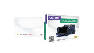
Additional hardware available. View our featured partner solutions.
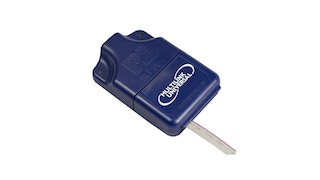
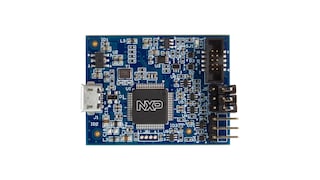
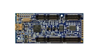
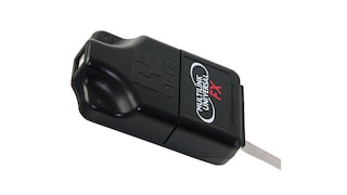
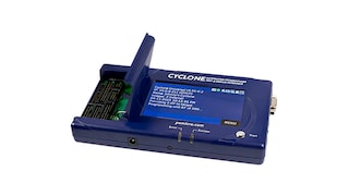
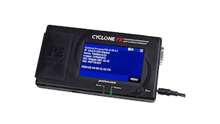
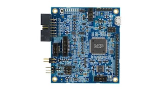
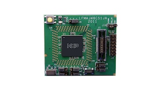
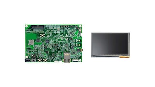

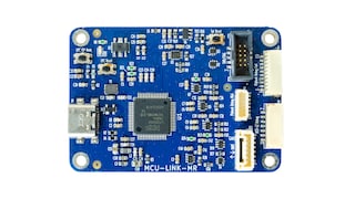
Sign in to access authorized secure files. Learn more about secure access rights.
1-5 of 12 hardware offerings
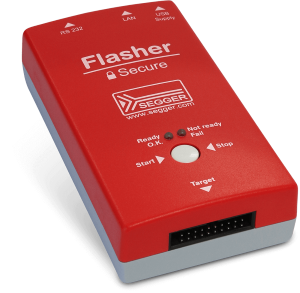
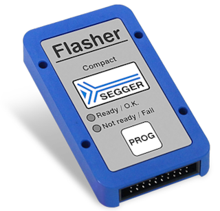
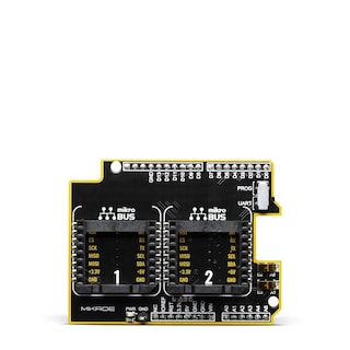
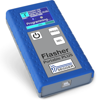
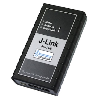
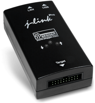
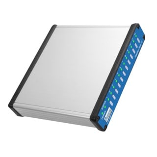
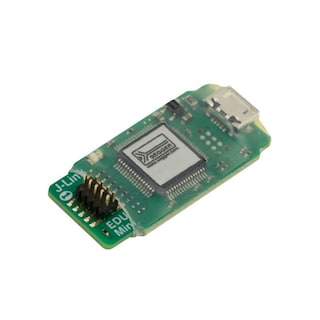
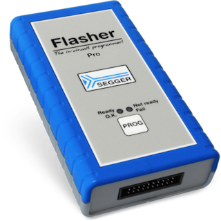

To find additional partner offerings that support this product, visit our Partner Marketplace.
1-5 of 14 hardware offerings


Additional hardware available. View our featured partner solutions.


Quick reference to our software types.
1-5 of 12 software files
Additional software available. View our featured partner solutions.
Note: For better experience, software downloads are recommended on desktop.
Sign in to access authorized secure files. Learn more about secure access rights.
Please wait while your secure files are loading.
1-5 of 37 software offerings
To find additional partner offerings that support this product, visit our Partner Marketplace.
1-5 of 12 software files
Additional software available. View our featured partner solutions.
Note: For better experience, software downloads are recommended on desktop.
1-5 of 18 engineering services


There are no results for this selection.
There are no results for this selection.
To find additional partner offerings that support this product, visit our Partner Marketplace.
4 trainings
Additional trainings are available. View our featured partner trainings.
4 trainings
Additional trainings are available. View our featured partner trainings.
9 trainings
To find additional partner offerings that support this product, visit our Partner Marketplace.
There are no recently viewed products to display.

Help us improve your experience on our site. We invite you to take our five-question survey.