Application Note (30)
-
LPC5460x Enhanced Image[AN13912]
-
LPC546xx SPIFI Usage and Performance[AN13165]
-
OTA update via TFTP on LPC5460x[AN13073]
Sign in for a personalized NXP experience.
Click over video to play
This is a modal window.
Beginning of dialog window. Escape will cancel and close the window.
End of dialog window.
This is a modal window. This modal can be closed by pressing the Escape key or activating the close button.
This is a modal window. This modal can be closed by pressing the Escape key or activating the close button.
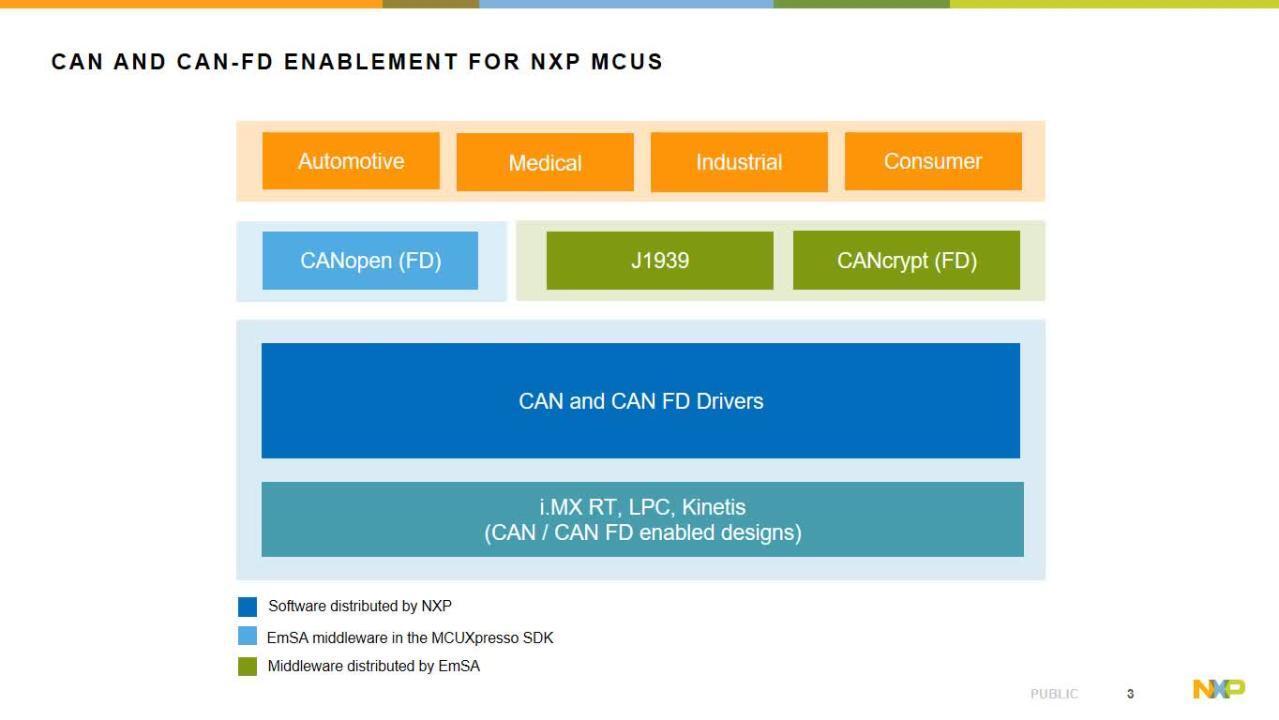
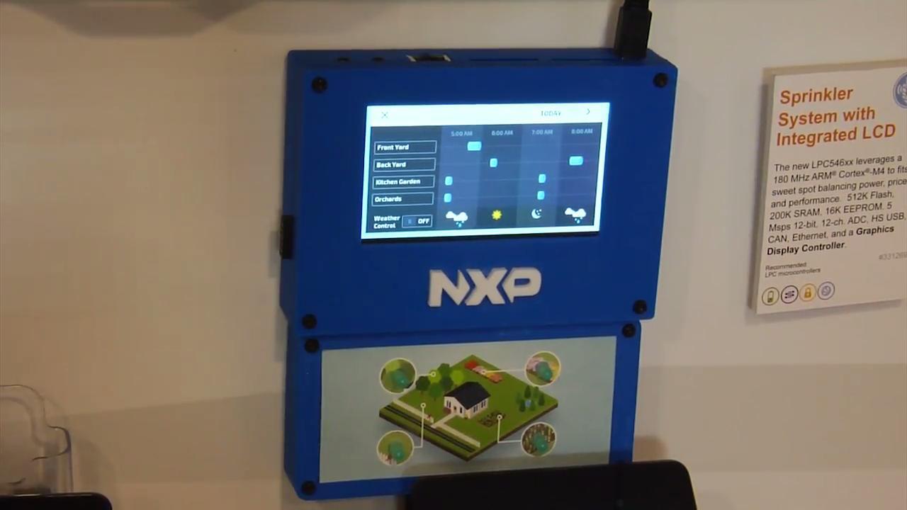
The LPC546xx MCU family combines the power efficiency of the 220 MHz Arm® Cortex®-M4 core with multiple high-speed connectivity options, advanced timers, and analog features. DSP capabilities enable LPC546xx MCU devices to support complex algorithms in data-intensive application. Providing flexibility with up to 512 KB Flash and external memory interfaces, this family provides the ability to adapt as requirements change. Flash options support large, flexible internal and external memory configurations. Compatibility within the LPC54000 series enables the LPC546xx MCU family to provide a seamless migration path for increasing processing power and adding the flexibility of additionally advanced peripherals.
This device is fully supported by NXP’s MCUXpresso Software and Tools, a comprehensive and cohesive set of free software development tools for Kinetis, LPC and i.MX RT microcontrollers. MCUXpresso SDK also includes project files for Keil MDK and IAR EWARM.

Note: To see the product features close this window.
| | | | | |
|---|---|---|---|---|---|
| | | | | |
| | | | | |
| | | | | |
| | | | | |
| | | | | |
| | | | | |
| | | | | |
| | | | | |
| | | | | |
| | | | | |
LPC546XXQuick reference to our documentation types.
1-10 of 47 documents
Compact List
There are no results for this selection.
Sign in to access authorized secure files. Learn more about secure access rights.
Please wait while your secure files are loading.
1-10 of 47 documents
Compact List
1-5of 6 design files
Sign in to access authorized secure files. Learn more about secure access rights.
Please wait while your secure files are loading.
1-5of 6 design files
1-5 of 10 hardware offerings
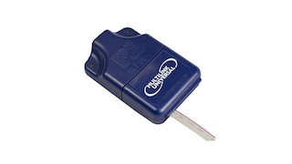
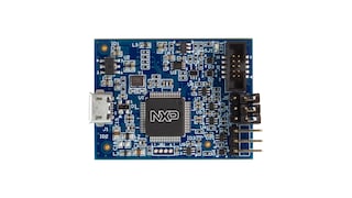
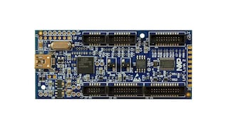
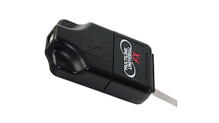
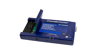
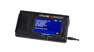
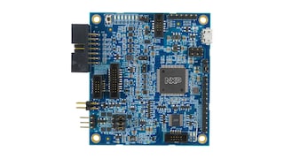
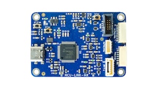
Sign in to access authorized secure files. Learn more about secure access rights.
1-5 of 10 hardware offerings


Quick reference to our software types.
1-5 of 16 software files
Additional software available. View our featured partner solutions.
Note: For better experience, software downloads are recommended on desktop.
Sign in to access authorized secure files. Learn more about secure access rights.
Please wait while your secure files are loading.
1-5 of 47 software offerings
To find additional partner offerings that support this product, visit our Partner Marketplace.
1-5 of 16 software files
Additional software available. View our featured partner solutions.
Note: For better experience, software downloads are recommended on desktop.
1-5 of 11 engineering services


There are no results for this selection.
There are no results for this selection.
To find additional partner offerings that support this product, visit our Partner Marketplace.
1-5 of 8 trainings
Additional trainings are available. View our featured partner trainings.
8 trainings
Additional trainings are available. View our featured partner trainings.
9 trainings
To find additional partner offerings that support this product, visit our Partner Marketplace.
There are no recently viewed products to display.
View or edit your browsing history