NFC Frontend supporting challenging RF environment for payment, physical access control

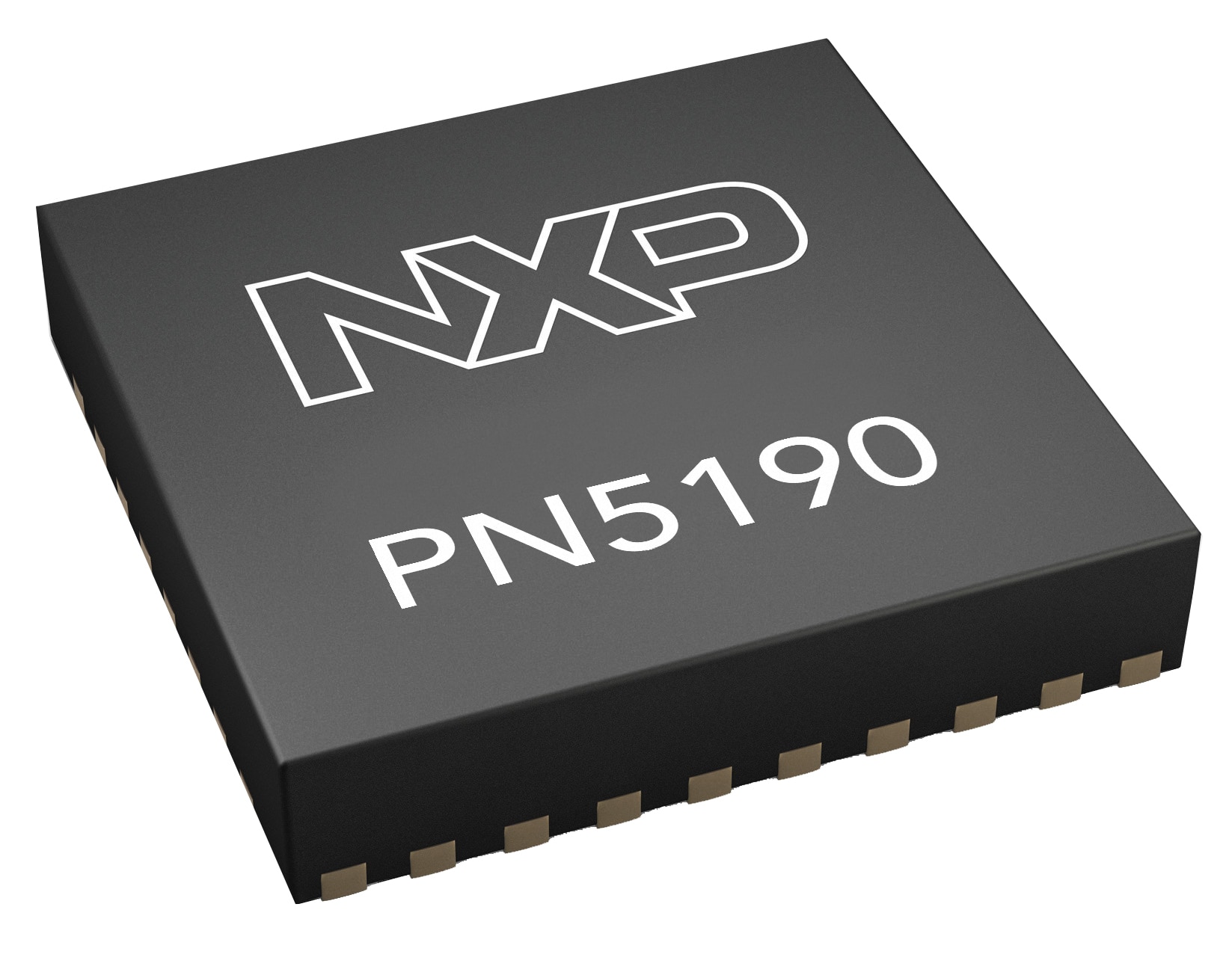
See product image

Block Diagram

PN5190 Block Diagram

PN5190 System Block Diagram

Features

  • High power (2W), feature-filled transmitter: DPC 2.0 (dynamic power control without processing load on host MCU)
  • Single 3.3 V supply with max TX transmitter power possible
  • Connection of 1 differential or 2 single-ended antennas
  • Robust receiver: Automatic configuration, advanced insensitivity against TFT display noise for higher RF performance
  • Full NFC Frontend with active load modulation in Card Mode for large operating distance
  • All relevant RF protocols implemented
  • NXP proprietary high datarates up to 212 Kbit for NTAG5 communication
  • Ultra-low-power card detect for low average current consumption
  • Flexible configuration of EMD handling (EMVCo 3.1, ISO, FeliCa) for future-proof system integration
  • Automatic antenna tuning (AAT) with variable capacitors
  • RF Debugging without external probing of test signals possible but not required – ideal debugging solution for PCI compliant POS terminals
  • Advanced RF debugging with AUX0, AUX1, AUX2 outputs
  • Certifications: EMVCo 3.1, NFC Forum
  • Supported by the NFC Cockpit Configuration Tool

Part numbers include: PN5190B2EV, PN5190B2HN.

Buy/Parametrics


Documentation

Quick reference to our documentation types.

1-5 of 14 documents

Show All

Design Files

Quick reference to our design files types.

3 design files

Hardware

Quick reference to our board types.

3 hardware offerings

Software

Quick reference to our software types.

1-5 of 18 software files

Show All

Note: For better experience, software downloads are recommended on desktop.

Engineering Services

5 engineering services

To find additional partner offerings that support this product, visit our Partner Marketplace.

Training

3 trainings

Support

What do you need help with?