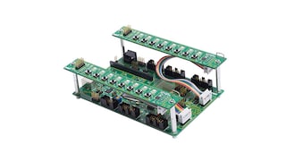
The PCA9665/PCA9665A serves as an interface between many standard parallel-bus microcontrollers/microprocessors
and the serial I²C-bus and allows the parallel bus system to communicate bidirectionally with the I²C-bus. The
PCA9665/PCA9665A can operate as a or a follower and can be a transmitter or receiver. Communication with the
I²C-bus is carried out on a Byte or Buffered mode using interrupt or polled handshake. The PCA9665/PCA9665A
controls all the I²C-bus specific sequences, protocol, arbitration and timing with no external timing element
required.
The PCA9665 and PCA9665A have the same footprint as the PCA9564 with additional features:
- 1 MHz transmission speeds
- Up to 25 mA drive capability on SCL/SDA
- 68-byte buffer
- I²C-bus General Call
- Software reset on the parallel bus


