
Product Longevity
Participating products are available for a minimum of 10 years. Designated participating products developed for the automotive, telecom and medical segments are available for a minimum of 15 years.
Sign in for a personalized NXP experience.
The MPC565 is a member of the MPC500 family of microprocessors that implements the Power Architecture® instruction standard architecture. The MPC565 is integrated with a floating point unit, an advanced peripheral set and 1 MB of flash memory on a single chip. This combination is ideal for high-performance automotive applications as well as other control-intensive applications.

Participating products are available for a minimum of 10 years. Designated participating products developed for the automotive, telecom and medical segments are available for a minimum of 15 years.
7 results
Exclude 7 NRND
Part | Order | CAD Model | Status | Package Type | Package Termination Count | Budgetary Price excluding tax |
|---|---|---|---|---|---|---|
End of Life | BGA388 | 388 | 10K @ US$100.43 | |||
End of Life | BGA388 | 388 | 10K @ US$95.65 | |||
End of Life | BGA388 | 388 | 10K @ US$100.43 | |||
End of Life | BGA388 | 388 | 10K @ US$109.99 | |||
End of Life | BGA388 | 388 | 10K @ US$75.28 - 10K @ US$109.99 | |||
End of Life | BGA388 | 388 | — | |||
End of Life | BGA388 | 388 | 10K @ US$99.99 - 10K @ US$100.24 |
MPC565Quick reference to our documentation types.
1-10 of 97 documents
Compact List
There are no results for this selection.
Please wait while your secure files are loading.
1-10 of 97 documents
Compact List
2 design files
Please wait while your secure files are loading.
2 design files
1-5 of 6 hardware offerings
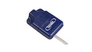
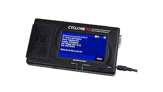
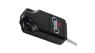
Additional hardware available. View our featured partner solutions.
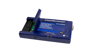
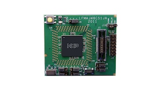

1 hardware offering
To find additional partner offerings that support this product, visit our Partner Marketplace.
1-5 of 6 hardware offerings


Additional hardware available. View our featured partner solutions.


Quick reference to our software types.
2 software files
Note: For better experience, software downloads are recommended on desktop.
Please wait while your secure files are loading.
1-5 of 14 software offerings
To find additional partner offerings that support this product, visit our Partner Marketplace.
2 software files
Note: For better experience, software downloads are recommended on desktop.
1-5 of 10 engineering services

.svg)


There are no results for this selection.
There are no results for this selection.
To find additional partner offerings that support this product, visit our Partner Marketplace.
4 trainings
To find additional partner offerings that support this product, visit our Partner Marketplace.
4 trainings
To find additional partner offerings that support this product, visit our Partner Marketplace.
There are no recently viewed products to display.
View or edit your browsing history
Help us improve your experience on our site. We invite you to take our five-question survey.