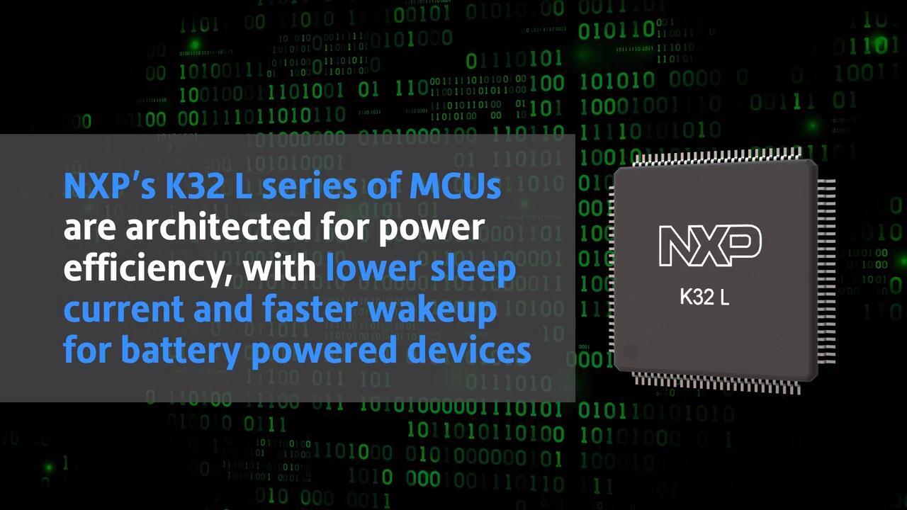
NXP’s Energy Efficient Cortex-M4 MCU with Cortex-M0+ and Advanced Security

Click over video to play

Block Diagram

K32 L3 MCU

K32 L3 MCU

Features

Core Processor

  • Arm Cortex-M4 core up to 72 MHz
  • Cortex-M0+ core up to 72 MHz

Memories

  • Up to 1.25 MB program flash memory
  • Up to 384 kB SRAM
  • 48 kB ROM with built-in secure boot loader

High Security

  • Cryptographic subsystem that includes a dedicated core, dedicated instruction memory (IRAM and IROM), and dedicated data RAM for autonomous implementation of encryption, signing, and hashing algorithms including AES-256, 3DES/DES, SHA-256, and RSA and ECC acceleration
  • Standalone True Random Number Generator (TRNG) with 512-bit of entropy and built-in statistical self-test
  • Secure key management for storing and protecting sensitive security keys
  • Wiping off the crypto subsystem memory including security keys upon sensing a security breach or physical tamper event
  • Resource domain controller for access control, system memory protection, and peripheral isolation
  • Built-in secure boot and secure over-the-air programming to assure only authorized and authenticated code runs on the device

Analog

  • 1 x 12-bit single ended low-power ADC
  • 2 x low-power comparator with 6-bit DAC
  • 1 x 12-bit low-power DAC
  • 1.2 V / 2.1 V dual-range voltage reference

Timers

  • Up to 2 x 6 ch., 2 x 2 ch. Timer/PWM Modules
  • Up to 2 x 4 ch. Low-Power Programmable Interrupt Timer
  • Up to 3 x Low-Power Timers
  • Real Time Clock (RTC)
  • 1 x 56-bit Timestamp

Peripherals

  • USB 2.0 Full-speed controller and transceiver
  • 1 x 32 ch. FlexIO supporting emulation of UART, I²C, SPI, I²S, Camera IF, LCD RGB, PWM/Waveform generation
  • Up to 4 x low-power UART
  • Up to 4 x low-power I²C
  • Up to 4 x 16-bit low-power SPI
  • 1 x EMVSIM module supporting the ISO-7816 protocol
  • 1 x Serial Audio Interface (SAI) with support for I²S and AC'97
  • 1 x Secure Digital Hardware Controller (uSDHC)
  • Parallel external FlexBus interface (RAM, ROM, simple follower devices)

Power Management

  • Bypass mode: 1.71 V to 3.6 V
  • Dual Output Buck DC-DC converter: 2.1 V to 3.6 V
  • Core voltage bypass: 1.14 V to 1.45 V direct supply to the core, bypassing internal regulator
  • Independent VDDIO1 and VDDIO2 supply: 1.71 V to 3.6 V
  • Independent VBAT (RTC): 1.71 to 3.6 V

Packages

  • 176 VFBGA, 9 mm x 9 mm x 0.86 mm, 0.5 mm pitch
  • 121 MBGA, 8 mm x 8 mm x 1.4 mm, 0.65 mm pitch
  • 100LQFP, 14 mm x 14 mm x 1.7 mm, 0.5 mm pitch
  • 64QFN, 9 mm x 9 mm x 0.85 mmx 0.5 mm pitch
  • 144 LQFP, 20 mm x 20 mm x 1.6 mm x 0.5 mm pitch

Buy/Parametrics


Documentation

Quick reference to our documentation types.

5 documents

Design Files

Hardware

Quick reference to our board types.

1-5 of 9 hardware offerings

Show All

Software

Quick reference to our software types.

5 software files

Note: For better experience, software downloads are recommended on desktop.

Engineering Services

5 engineering services

To find additional partner offerings that support this product, visit our Partner Marketplace.

Training