8-bit Segment LCD LL MCUs

Block Diagram

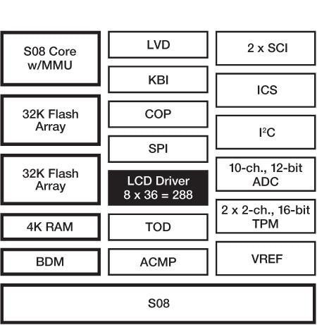
S08LL Microcontroller Block Diagram

S08LL Microcontroller Block Diagram

Features

S08 Central Processor Unit (CPU)

  • Up to 40 Mhz CPI at 3.6V to 2.1V
  • Up to 20 MHz CPU at 2.1V to 1.8V across temperature range of -40°C to +85°C
  • HCS08 instruction set with added BGND instruction

Enablement and Development Support

  • Low-cost, reconfigurable Tower® evaluation and demonstration platform
  • Breakpoint capability
  • ICE debug module
    • three comparators and nine trigger modes
    • Eight deep FIFO for storing change-of-flow addresses and event-only data
    • supports both tag and force breakpoints.
  • Migration path from smaller flash size devices (LL16)

Power-Saving Features

  • Two ultra-low-power stop modes, one of which allows limited use of peripherals
  • New low-power run and wait modes
  • 6 µs typical wake-up time from stop mode
  • Internal clock source (ICS) module containing a frequencylocked loop (FLL) controlled by internal or external reference
  • Ultra-low-power oscillator (OSC)
  • Clock gating disables clocks to unused peripherals

LCD Driver and Internal Charge Pump

  • Integrated LCD driver supports both standard 3V and 5V LCD glass
  • Configurable display for 8 x 36 or 4 x 40 segment display
  • Low-power blinking mode
  • Internal charge pump
  • Front plane (FP) and back plane (BP) re-assignments
  • Capable of running in STOP3 and STOP2 mode
  • LCD driver pins are muxed with GPIO and other functions

On-Chip Memory

  • Up to 64 KB flash compromised of two separate arrays to facilitate read/program/erase over full operating voltage and temperature
  • 1.8V to 3.6V RAM

Peripherals

  • Analog-to-digital converter (ADC)
    • Up to 10-channel
    • 12-bit resolution
    • 2.5 µs conversion time
    • Automatic compare function
    • Internal temperature sensor
    • Internal bandgap reference channel
    • Operation in stop mode
  • Timer
    • Two 2-channel (TPM1 and TPM2)
    • Selectable input capture
    • Output compare
    • Buffered-edge or center-aligned PWM on each channel
  • Two serial communications interfaces (SCI) modules
    • Asynchronous communications
    • 13-bit break option
    • Flexible baud rate generator
    • Double buffered transmit and receive and optional HW parity checking and generation
  • Time of day (TOD) 8-bit
    • Quarter second counter with match register
    • External clock source for precise time base
    • Calendar
    • Task scheduling functions
  • Serial peripheral interface (SPI) module
    • Full-duplex or single-wire bidirectional
    • Double-buffered transmit and receive leader or follower mode
    • MSB-first or LSB first shifting
  • I²C with up to 100 kbps with maximum bus loading
    • Multicontroller operation
    • Programmable target address
    • Interruptdriven byte-by-byte data transfer
    • Support for broadcast mode and 10-bit addressing

Input/Output

  • Up to 39 general purpose input/output (GPIO)
  • Two output-only pins
  • Eight keyboard interrupt (KBI) pins with selectable polarity

System Protection

  • Watchdog computer operating properly (COP) reset with option to run from dedicated 1 kHz internal clock source or bus clock
  • Low-voltage detection with reset or interrupt, selectable trip points
  • Illegal op code and illegal address detection with reset
  • Flash block protection

Buy/Parametrics


Documentation

Quick reference to our documentation types.

1-5 of 41 documents

Show All

Design Files

Quick reference to our design files types.

2 design files

Hardware

Quick reference to our board types.

1-5 of 6 hardware offerings

Show All

Software

Quick reference to our software types.

1-5 of 10 software files

Show All

Note: For better experience, software downloads are recommended on desktop.

Engineering Services

2 engineering services

To find additional partner offerings that support this product, visit our Partner Marketplace.

Support