Design Files
1 design file
Receive the full breakdown. See the product footprint and more in the eCad file.
-
Calculators
S08 Battery Calculator
The MC9S08GT family are cost-effective, high-performance S08 general purpose 8-bit microcontrollers. All MCUs in the family use the enhanced S08 core and are available with a variety of modules, memory sizes, memory types and package types.
Additionally, the MC9S08GT16A and MC9S08GT8A series of microcontrollers further extend the GT family to smaller memory sizes, while maintaining higher end functionality often associated with more expensive parts. MC9S08GT16A doubles the RAM of its predecessor. An additional option is offered for those customers requiring an 8 KB flash part.
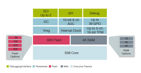
Note: To see the product features close this window.
Part numbers include: MC9S08GT16ACFBE, MC9S08GT16ACFCE, MC9S08GT16ACFDE, MC9S08GT16AMFBE, MC9S08GT16AMFCE, MC9S08GT32ACFBE, MC9S08GT32ACFDE, MC9S08GT60ACFBE, MC9S08GT60ACFDE, MC9S08GT8ACFBE, MC9S08GT8ACFCE, MC9S08GT8AMFBE, MC9S08GT8AMFCE, MC9S08GT8AMFDE.
|
|
|
|
|
|
|
|---|---|---|---|---|---|
|
|
|
|
|
|
|
|
|
|
|
|
|
|
|
|
|
|
|
|
|
|
|
|
|
|
|
|
|
|
|
|
|
|
|
|
|
|
|
|
|
|
|
|
|
|
|
|
|
|
|
|
|
|
|
|
|
|
|
|
|
|
|
|
|
|
|
|
|
|
Quick reference to our documentation types.
1-5 of 70 documents
Please wait while your secure files are loading.
1 design file
Receive the full breakdown. See the product footprint and more in the eCad file.
Please wait while your secure files are loading.
1-5 of 6 hardware offerings
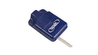

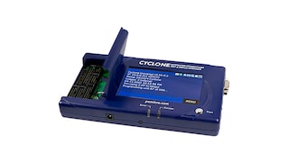
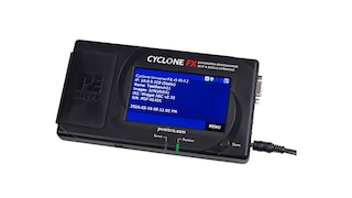

Quick reference to our software types.
1-5 of 12 software files
Additional software available. View our featured partner solutions.
Note: For better experience, software downloads are recommended on desktop.
Please wait while your secure files are loading.
1 software offerings

To find additional partner offerings that support this product, visit our Partner Marketplace.
2 engineering services

.svg)
There are no results for this selection.
To find additional partner offerings that support this product, visit our Partner Marketplace.