
Product Longevity
Participating products are available for a minimum of 10 years. Designated participating products developed for the automotive, telecom and medical segments are available for a minimum of 15 years.
The PCA9685 is an I²C-bus controlled 16-channel LED controller optimized for Red/Green/Blue/Amber (RGBA) color backlighting applications. Each LED output has its own 12-bit resolution (4096 steps) fixed frequency individual PWM controller that operates at a programmable frequency from a typical of 24 Hz to 1526 Hz with a duty cycle that is adjustable from 0 % to 100 % to allow the LED to be set to a specific brightness value. All outputs are set to the same PWM frequency.
Each LED output can be off or on (no PWM control) or set at its individual PWM controller value. The LED output driver is programmed to be either open-drain with a 25 mA current sink capability at 5 V or totem pole with a 25 mA sink, 10 mA source capability at 5 V. The PCA9685 operates with a supply voltage range of 2.3 V to 5.5 V and the inputs and outputs are 5.5 V tolerant. LEDs can be directly connected to the LED output (up to 25 mA, 5.5 V) or controlled with external drivers and a minimum amount of discrete components for larger current or higher voltage LEDs.
The PCA9685 is in the new Fast-mode Plus (Fm+) family. Fm+ devices offer higher frequency (up to 1 MHz) and more densely populated bus operation (up to 4000 pF).
Although the PCA9635 and PCA9685 have many similar features, the PCA9685 has features that make it more suitable for applications such as LCD or LED backlighting and Ambilight:
The active LOW Output Enable input pin (OE) allows asynchronous control of the LED outputs and can be used to set all the outputs to a defined I²C-bus programmable logic state. The OE can also be used to externally ‘pulse width modulate’ the outputs, which is useful when multiple devices need to be dimmed or blinked together using software control.
Software programmable LED All Call and three Sub Call I²C-bus addresses allow all or defined groups of PCA9685 devices to respond to a common I²C-bus address, allowing, for example, all red LEDs to be turned on or off at the same time or marquee chasing effect, thus minimizing I²C-bus commands. Six hardware address pins allow up to 62 devices on the same bus.
The Software Reset (SWRST) General Call allows the controller to perform a reset of the PCA9685 through the I²C-bus, identical to the Power-On Reset (POR) that initializes the registers to their default state causing the outputs to be set LOW. This allows an easy and quick way to reconfigure all device registers to the same condition via software.
Participating products are available for a minimum of 10 years. Designated participating products developed for the automotive, telecom and medical segments are available for a minimum of 15 years.
2 results
Include 0 NRND
Part | Order | CAD Model | Status | Number of Channels | Output Current on pin LEDn (Max) (mA) | Supply Voltage [Min to Max] (V) | Topology | Blinking Rate (Min to Max) (Hz) | # of Addresses | Operating Temperature (Min-Max) (℃) | AEC-Q100 compliant | Package Type | Package Dimensions (LxWxZ (mm)) | Budgetary Price excluding tax |
|---|---|---|---|---|---|---|---|---|---|---|---|---|---|---|
Active | 16 | 25 | 2.3 to 5.5 | Voltage switch | 24 to 1526 | 64 | -40 to 85 | N | HVQFN28 | 6 x 6 x 0.85 | 1K @ US$1.13 | |||
Active | 16 | 25 | 2.3 to 5.5 | Voltage switch | 24 to 1526 | 64 | -40 to 85 | N | TSSOP28 | 4.4 x 9.7 x 0.9 | 1K @ US$1.12 - 1K @ US$1.06 |
Quick reference to our documentation types.
1-10 of 13 documents
Compact List
1-10 of 13 documents
Compact List
2 design files
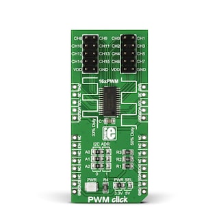
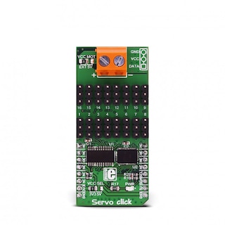
4 hardware offerings
To find additional partner offerings that support this product, visit our Partner Marketplace.
There are no recently viewed products to display.
