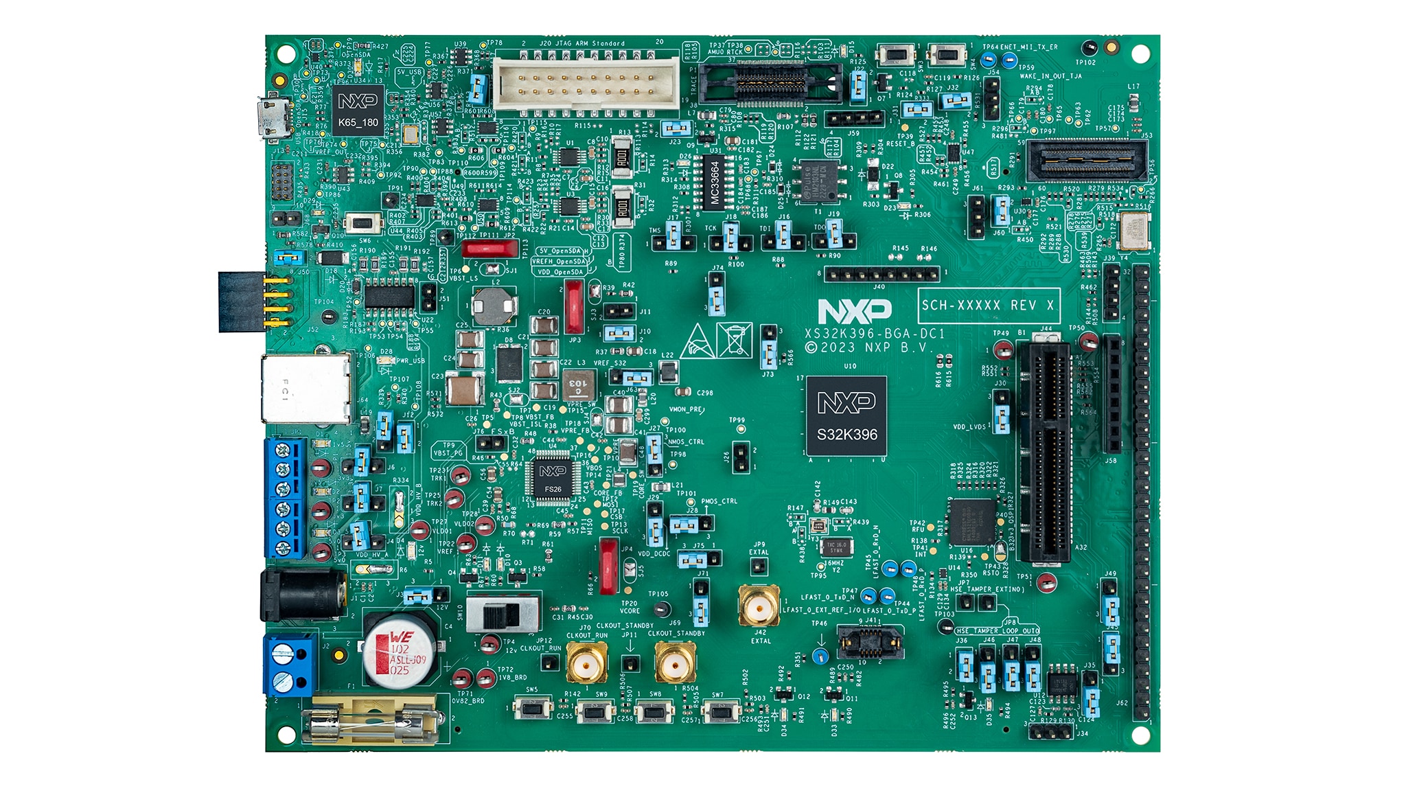
Getting Started With S32K396-BGA-DC1 Evaluation Board
Contents of this document
-
Out of the Box
-
Get Software
-
Plug It In
Sign in to save your progress. Don't have an account? Create one.
Purchase your S32K39/37/36 Electrification Microcontrollers Evaluation Board

2. Get Software
2.1 Download and install the latest S32DS
Download and install S32 Design Studio IDE for S32 Platform. Click S32 Design Studio for S32 Platform v.3.5.
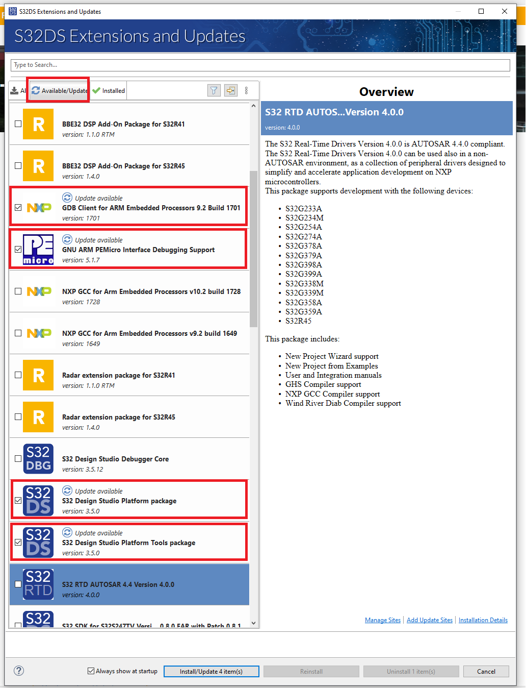
2.2 Update the S32 Design Studio
- Run the design Studio
- Go to the menu and click on Help/S32DS Extensions and Updates
- Select Available updates and install all with blue update icon
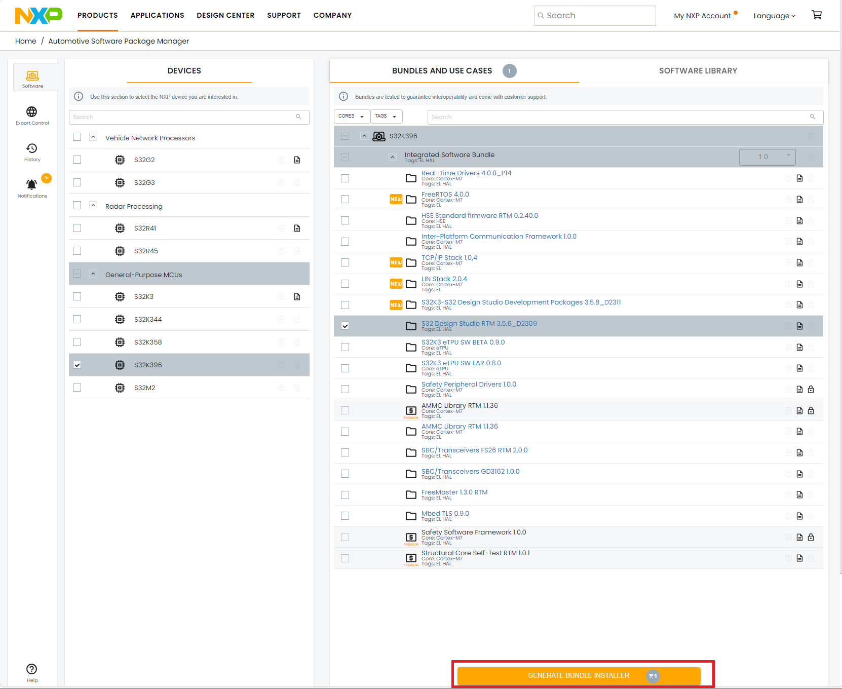
2.3 Download and Install the S32K396 Development Package
- Install the S32K39 Software bundle from the Automotive Software Package Manager
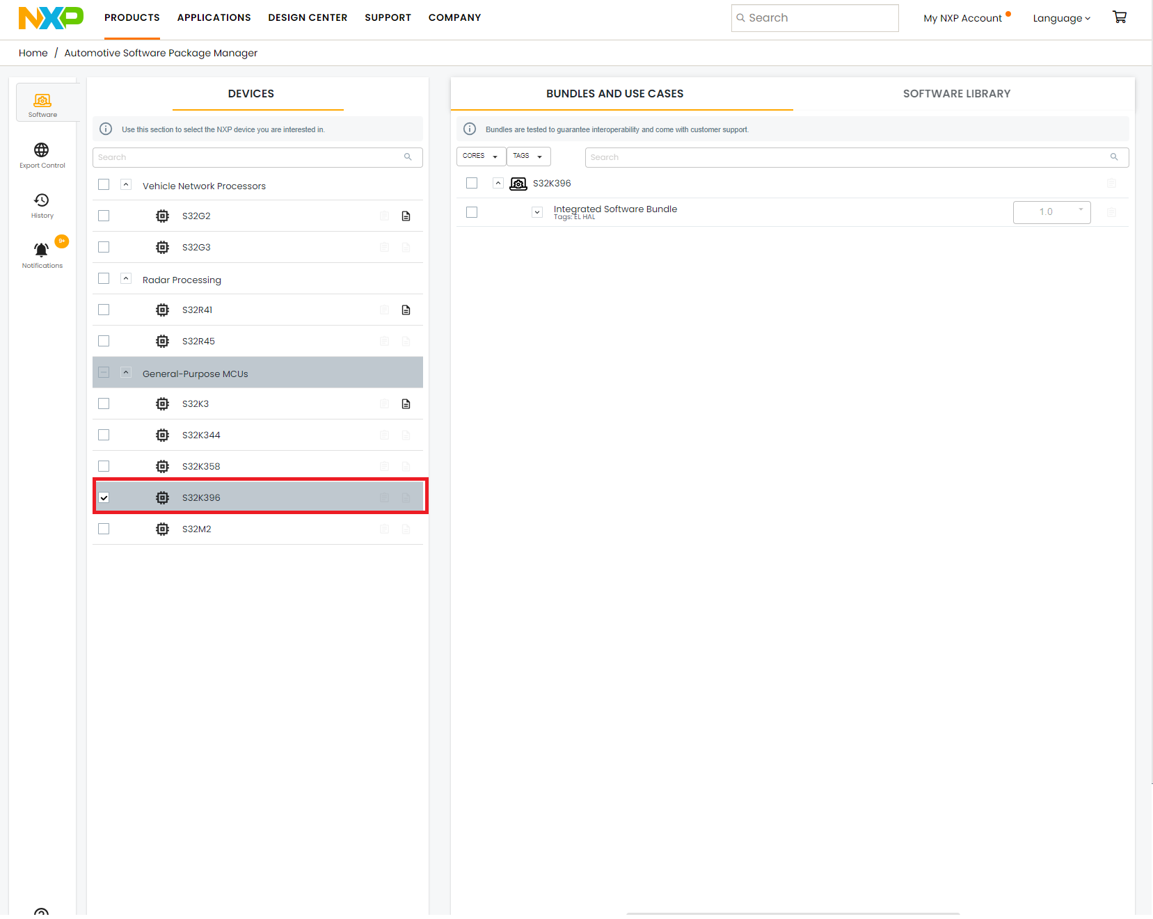
- Open the Integrated Software Bundle and select S32 Design Studio RTM 3.5.6_D2309
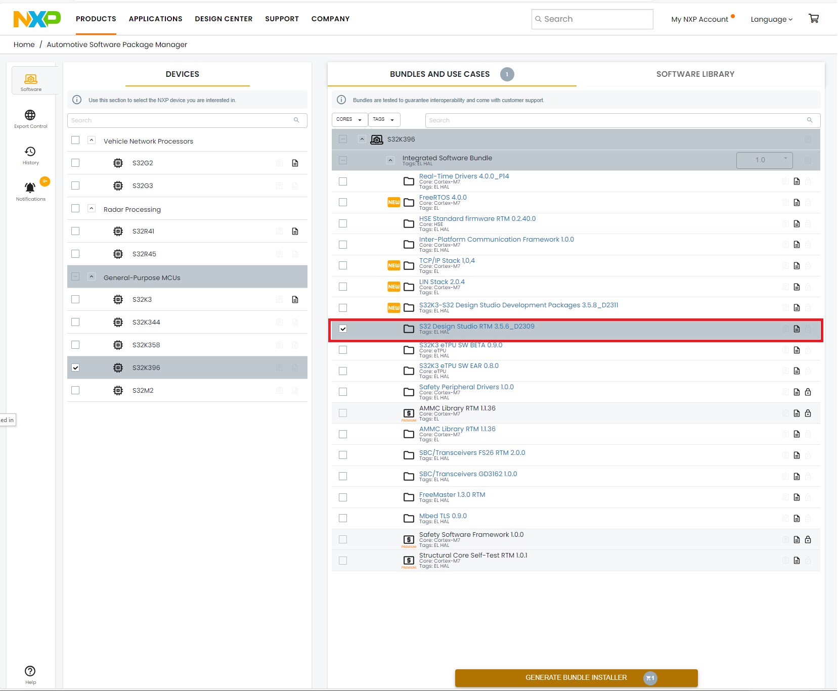
- Click on Generate Bundle Installer and following the instruction
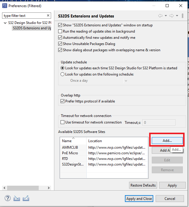
2.4 Install the S32K3xx Development Package and RTD
- Go to the menu and click on Help/S32DS Extensions and Updates
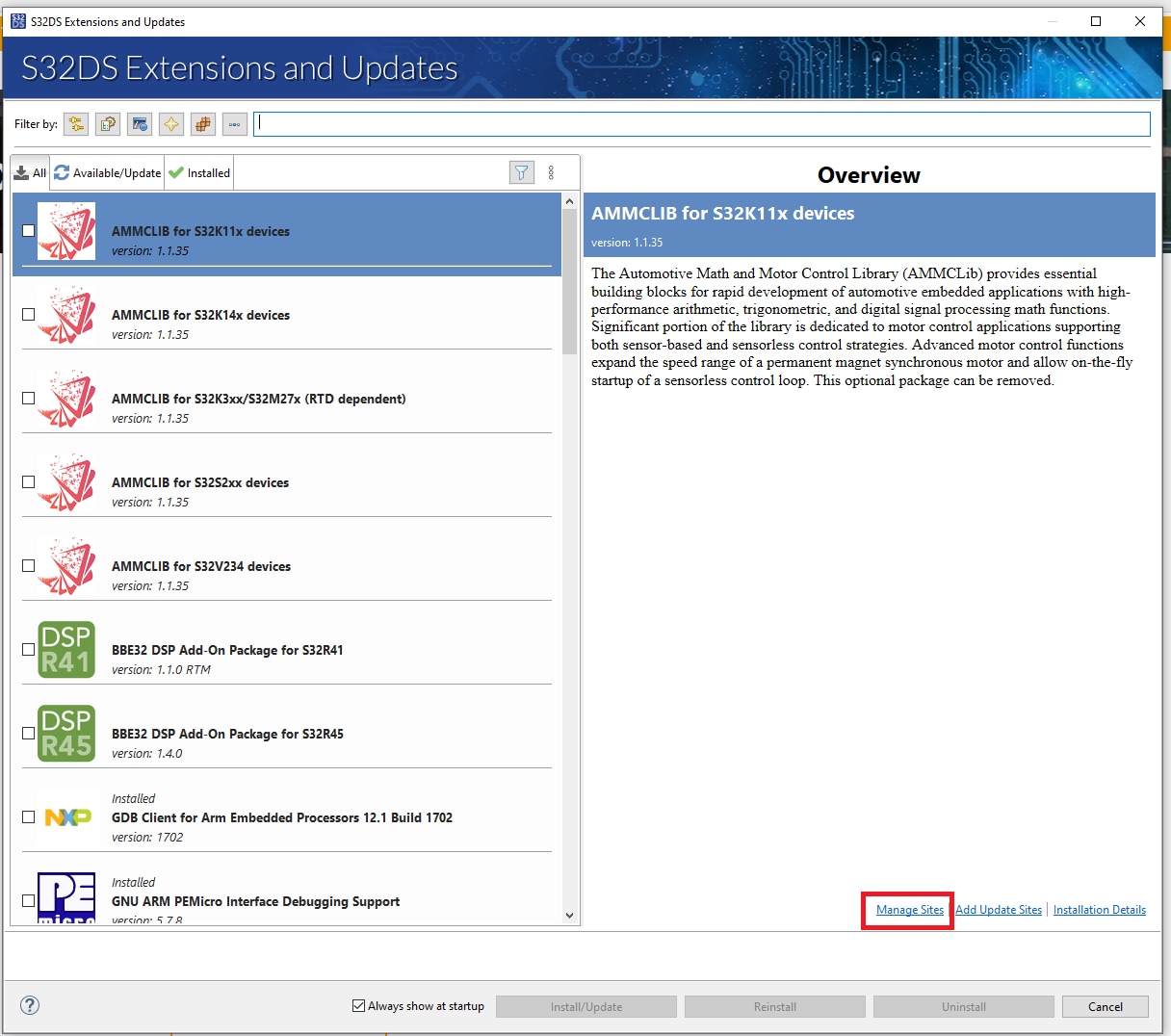
- Click on Manage Site
- Click Add button
- Click on the Archive button and select the downloaded K396 development package archive file
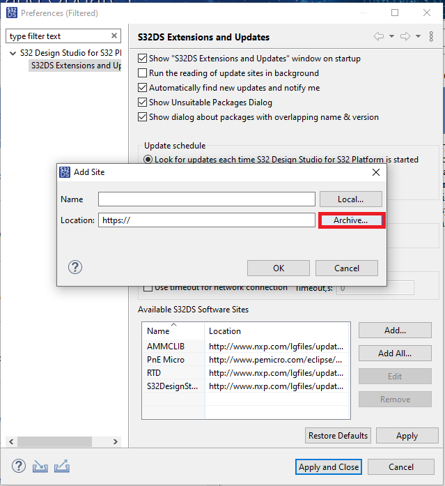
- Click OK
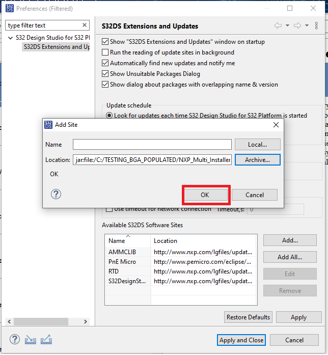
- Click apply and close
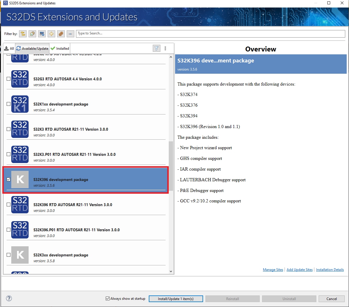
- Select and install the S32K396 development package
2.5 Install the RTD Drivers
- Go to the menu and click on Help/S32DS Extensions and Updates
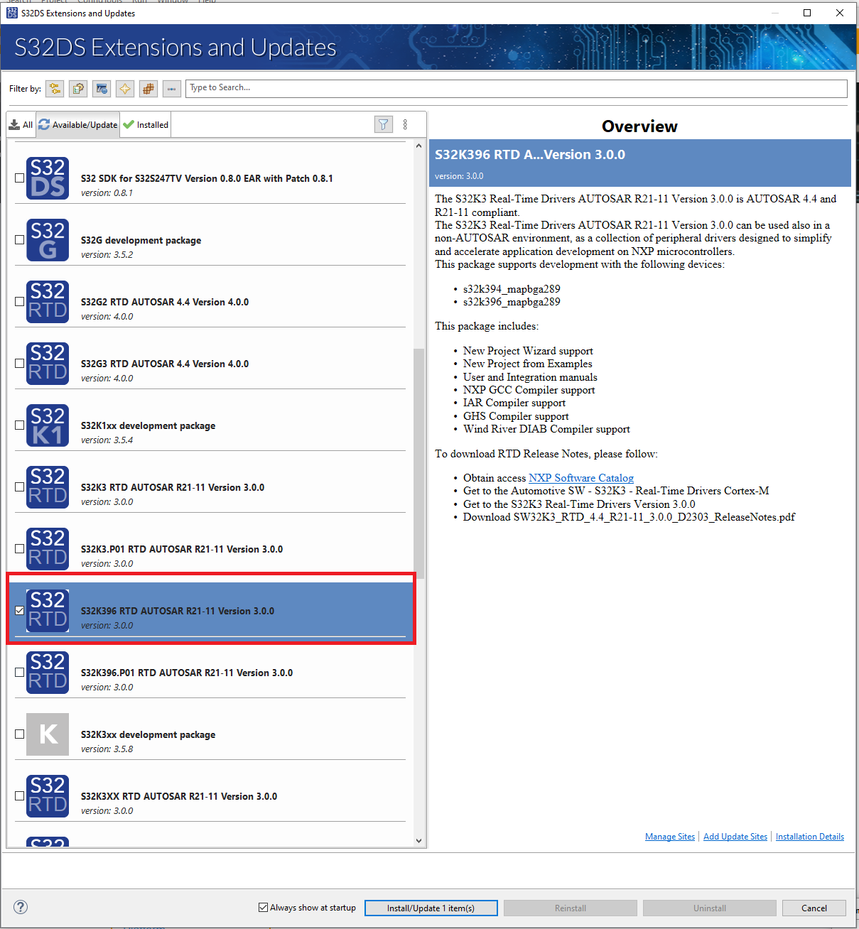
- Select the S32K396 RTD AUTOSAR® R21-11 Version 3.0.0 and install it
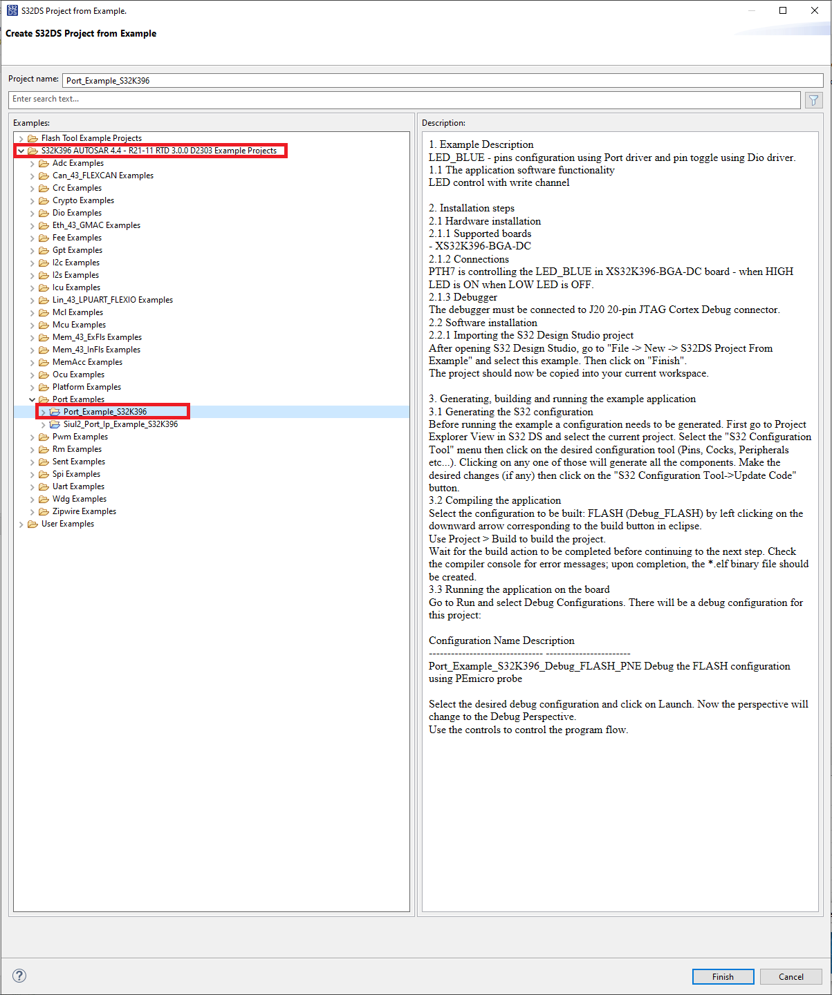
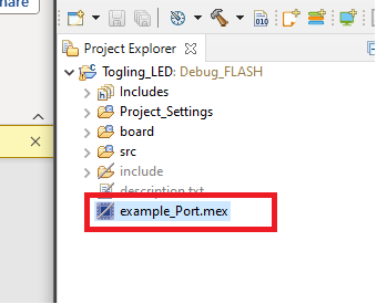
2.6 Create the Project for LED D35
- Go to menu and click New/S32DS Project from Example

- Open the S32K396 AUTOSAR 4.4 - R21-11 RTD 3.0.0 D2303 Example Projects and select Port_Example_S32K396
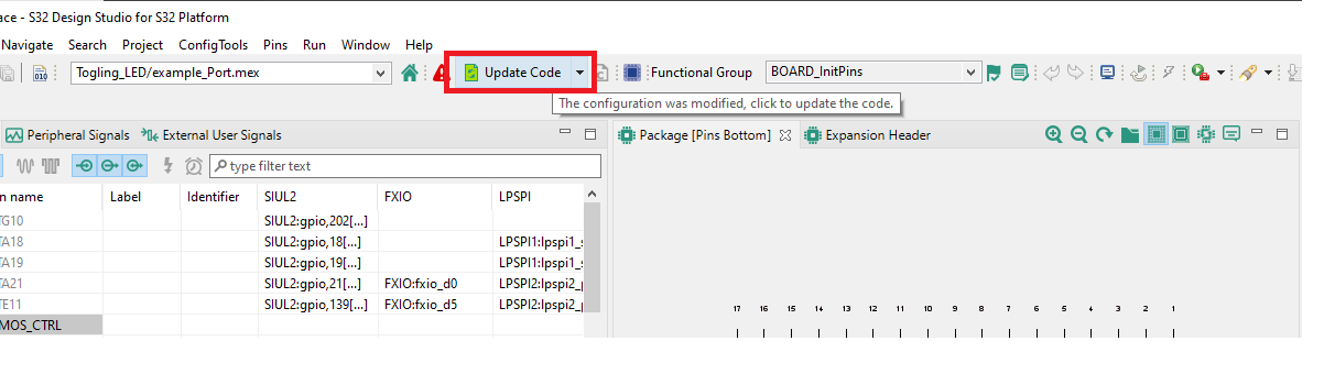
- Open the mex file to generate the RTD necessary files
- Click on update the code
- Go back into the source code view
- Build the project by clicking o the hammer icon
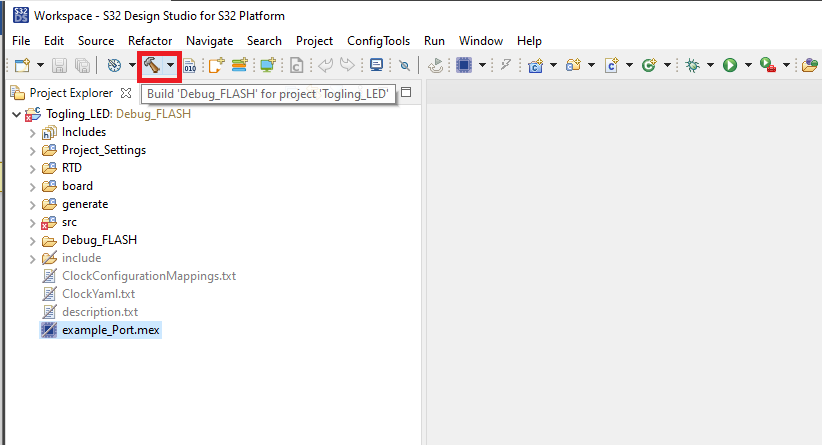
2.7 Program the Code Into the Board
-
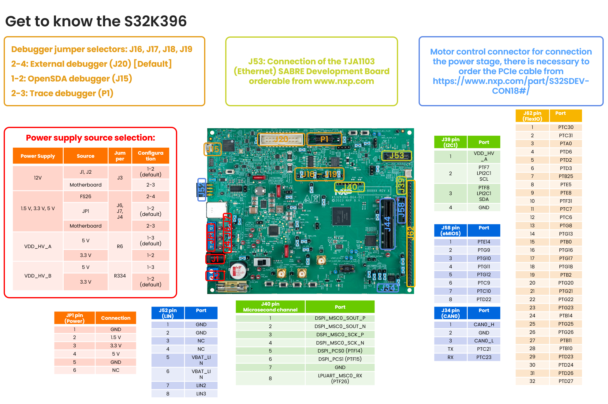
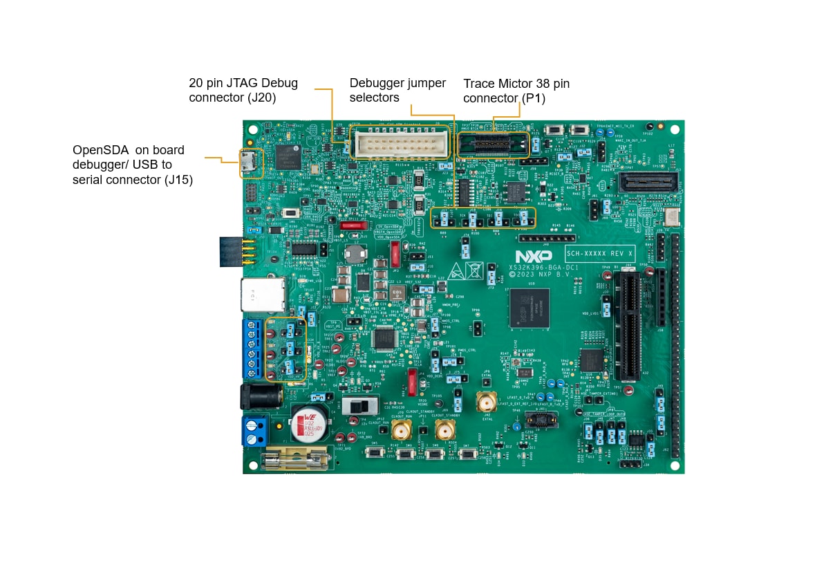
By External debugger
- The board is by default to configure to use external debugger connected to the
J20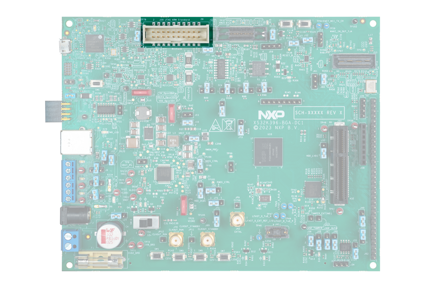
- Connect your external debugger and program the elf generated by the S32DS
- The board is by default to configure to use external debugger connected to the
-
Using on board OpenSDA debugger
- Change debugger selection jumpers to use OpenSDA (
J16,J17,J18,J19position 1-2)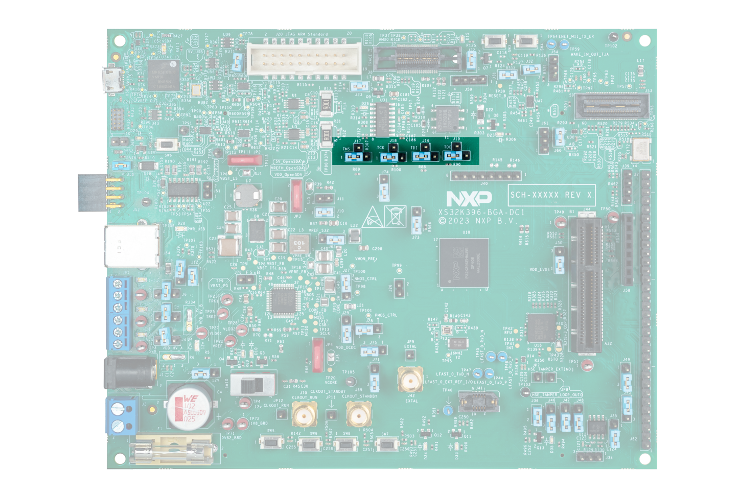
- Connect the board with PC by USB cable and power and plug 12 V power supply to the board. Plug the power supply to the board when the
SW10is I the OFF position and after the 12 V is applied turn in to ON position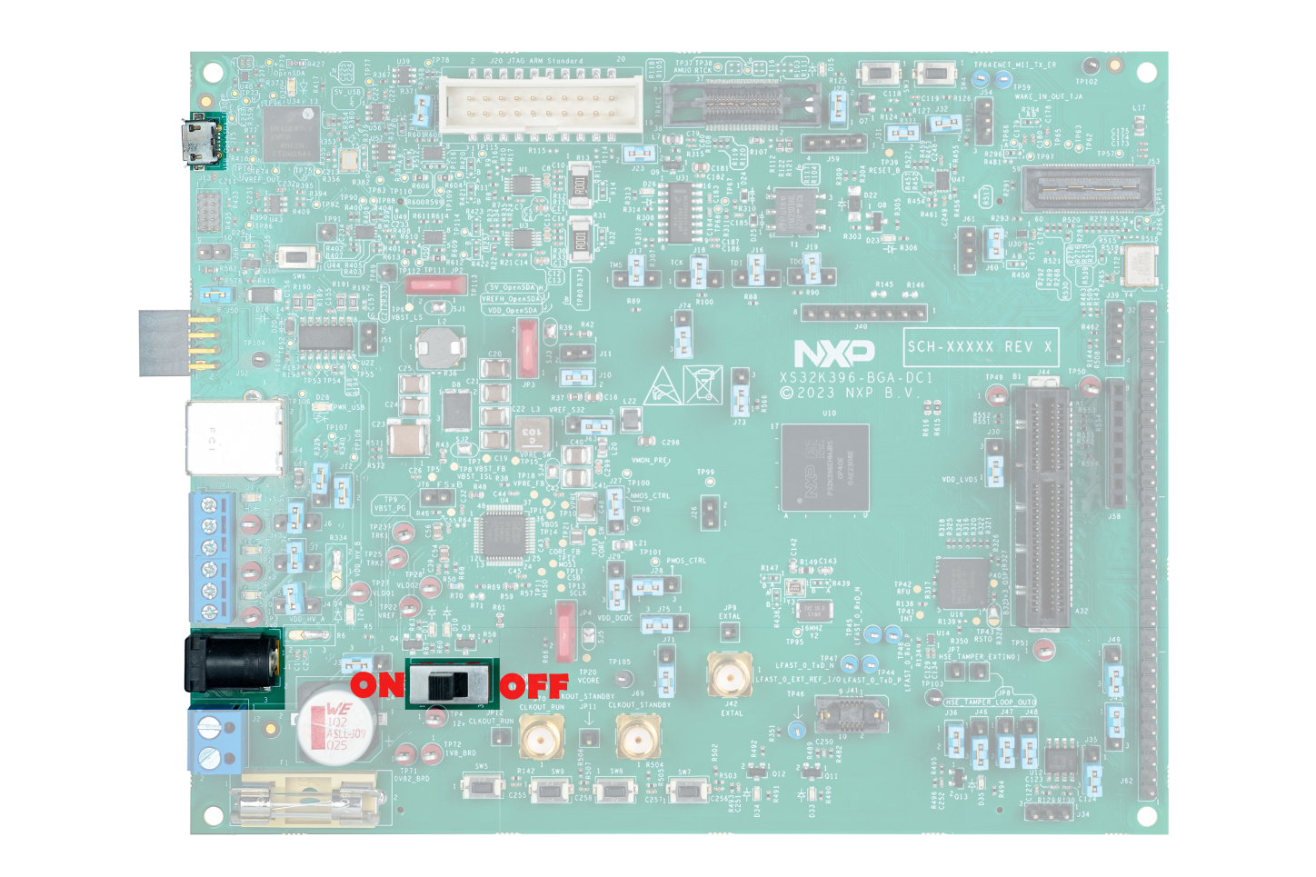
- Go back to the design studio and click on the debug icon and select debug configuration
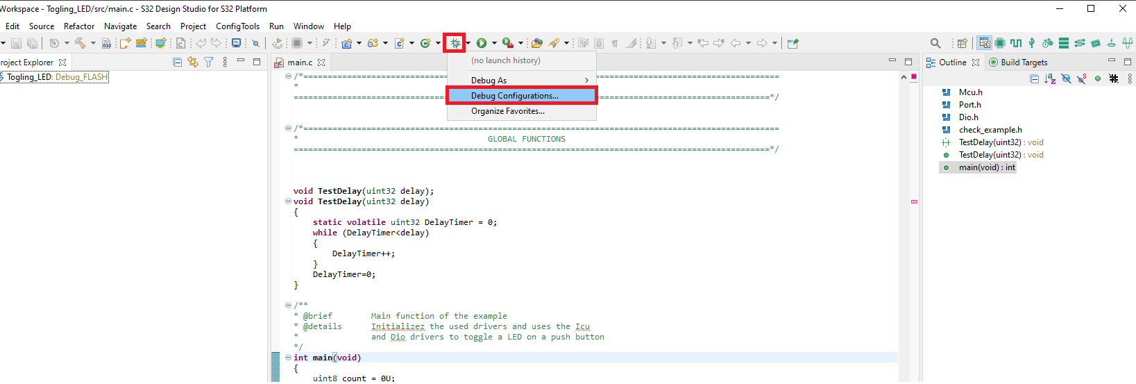
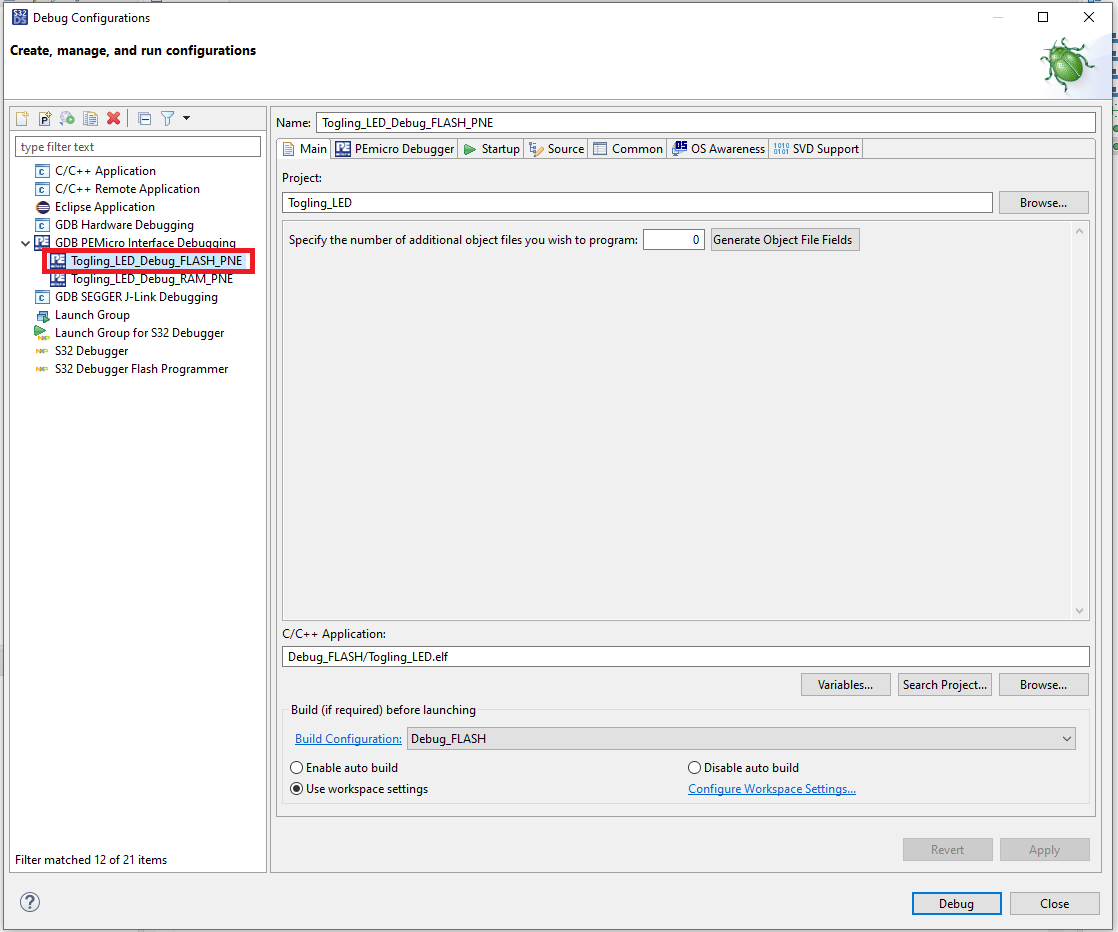
- Select GDB PEMicro Interface Debugging/xxx_Debug_FLASH_PNE, where xxx is name of the project when you created it from the example
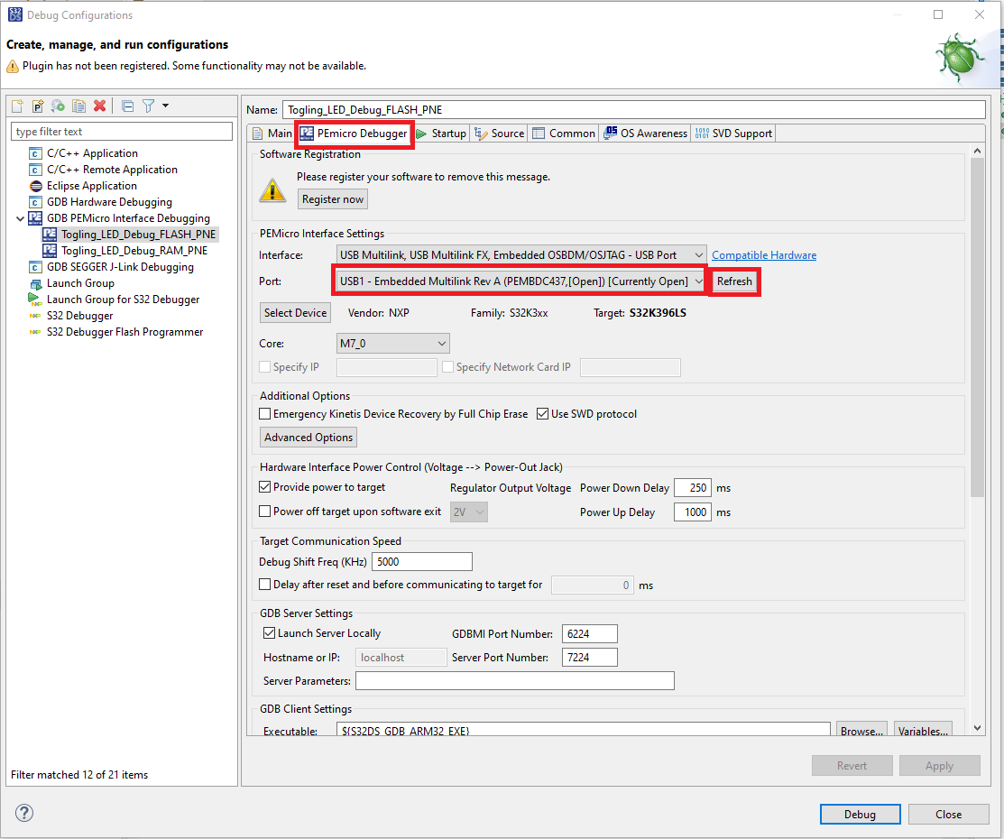
- Select PEmicro Debugger when there is not any device seen in the Port click on the refresh button
- Click on the debug button

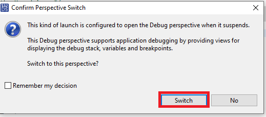
- Click on switch button to go to the debugger view
- Click on the run button I the debugger window
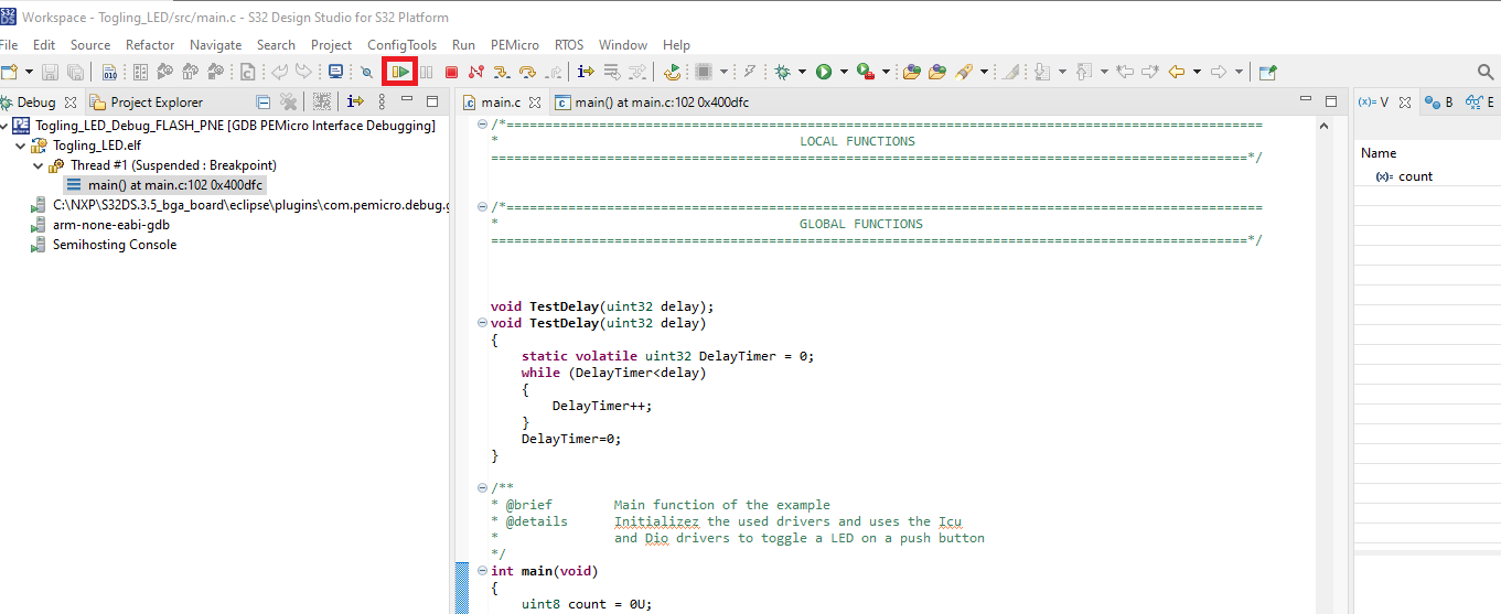
- You will see the
D35blink 10 times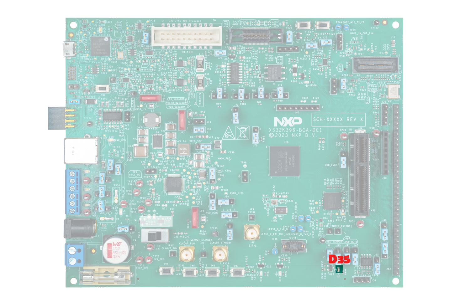
- Change debugger selection jumpers to use OpenSDA (
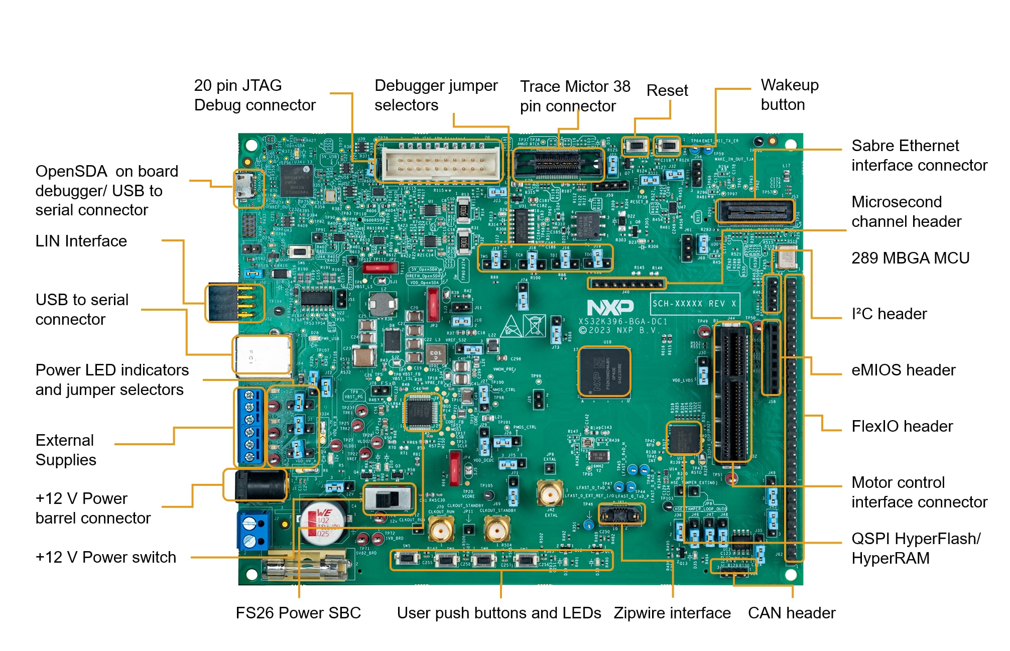
3. Plug It In
3.2 Plug in the Debugger
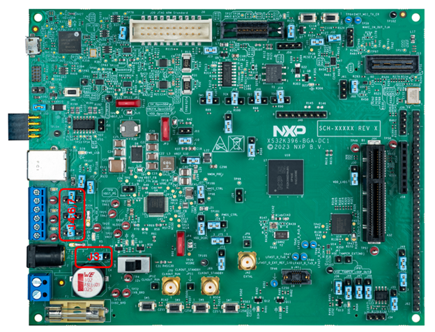
| Jumper | Configuration | Selection of |
|---|---|---|
J3 |
1-2 (default) | Source of the 12 V power supply |
J4 |
2-4 | Source of the 5 V power supply |
J6 |
2-4 | Source of the 1.5 V power supply |
J7 |
2-4 | Source of the 3.3 V power supply |
The S32K396 BGA DC1 supports three different debuggers but just one can be used in the same time by configuring the jumpers J16, J17, J18 and J19. By default the board is configured to use an external debugger plug in into the connector J20.
The debugger selection table.
| Debugger | J16, J17, J18, J19 Configuration |
|---|---|
On board (J15) |
1-2 |
External (J20) |
2-4 (default) |
External Trace (P1) |
2-3 |
3.3 How to Get Started
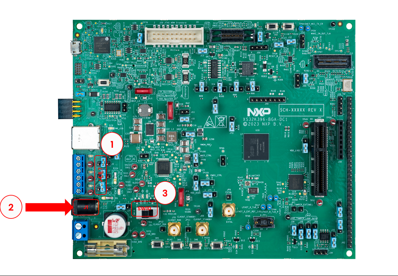
- Change the position of the
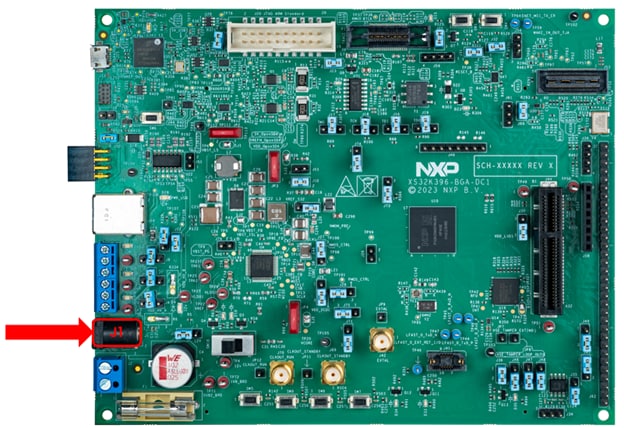
J6,J7,J4to position 2-4 (MCU power supply generated by the FS26 device) - Connect the external power supply 12 V to jack connector
J1 - Turn on the main switch
SW10to power on the board
3.4 Configure Jumpers for the S32K396-BGA-DC1 Evaluation Board
Before, plug in the power supply switch of the SW10 (position 3):
The S32K396 BGA DC1 supports three different debuggers but just one can be used in the same time by configuring the jumpers J16, J17, J18 and J19. By default is the board is configured to use an external debugger plug in into the connector J20.
The debugger selection table.
| Debugger | J16, J17, J18, J19 Configuration |
|---|---|
On board (J15) |
1-2 |
External (J20) |
2-4 (default) |
External Trace (P1) |
2-3 |
For powering, the power supply adapter (12 V output) will be used, which is part of the delivery and will be plugged into J1.
Before, plug in the power supply switch of the SW10 (position 3):
Plug in 12 V power Supply to J1:
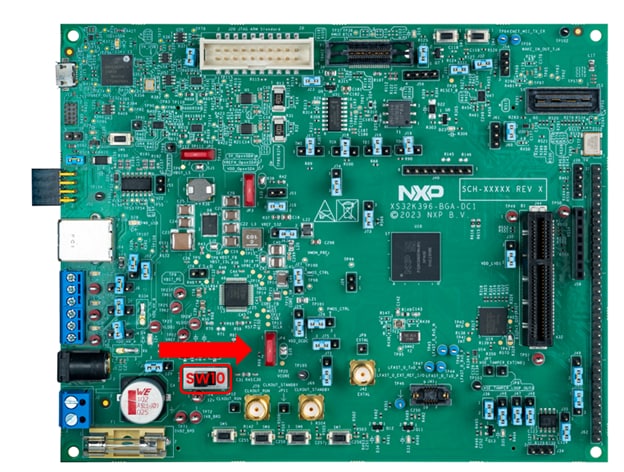
Switch on the SW10 (position 1):
Design Resources
Software
- Automotive Software Package Manager
- S32K3 Standard Software
- S32K3 Reference Software
- S32 Design Studio for S32 Platform
- Inter-Platform Communication Framework (IPCF)
- S32 Safety Software Framework (SAF) and Safety Peripheral Drivers (SPD)
- Structural Core Self-Test (SCST) Library
- Model-Based Design Toolbox (MBDT)
- Motor Control Application Tuning (MCAT) Tool
- S32 Design Studio IDE
- FreeMASTER Run-Time Debugging Tool
- Automotive Math and Motor Control Library (AMMCLib)
Support
How can we help you? Whether you are looking for assistance on a complex design challenge or some quick advice, NXP offers a variety of support options to suit your needs.
On this page
- 2.1
Download and install the latest S32DS
- 2.2
Update the S32 Design Studio
- 2.3
Download and Install the S32K396 Development Package
- 2.4
Install the S32K3xx Development Package and RTD
- 2.5
Install the RTD Drivers
- 2.6
Create the Project for LED D35
- 2.7
Program the Code Into the Board