A3G26H501W17S|2496-2690 MHz, 56 W Avg, 48 V | NXP Semiconductors

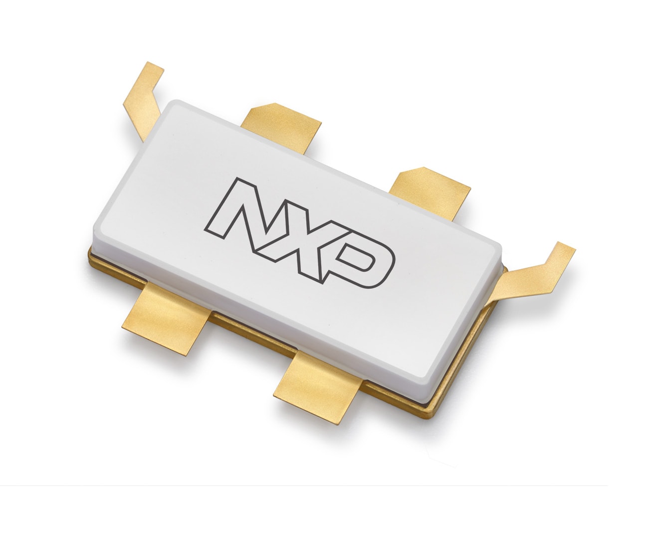
A3G26H501W17S 2496-2690 MHz, 56 W Avg., 48 V Airfast® RF Power GaN Transistor

See product image

Product Details

Features

  • High terminal impedances for optimal broadband performance
  • Advanced high performance in-package Doherty
  • Improved linearized error vector magnitude with next generation signal
  • Able to withstand extremely high output VSWR and broadband operating conditions
  • RoHS compliant

RF Performance Table

2600 MHz

Typical Doherty Single-Carrier W-CDMA Characterization Performance: VDD = 48 Vdc, IDQA = 350 mA, VGSB = –5.0 Vdc, Pout = 56 W Avg., Input Signal PAR = 9.9 dB @ 0.01% Probability on CCDF. (1)
Frequency Gps
(dB)
ηD
(%)
P3dB
(dBm) (2)
ACPR
(dBc)
2496 MHz14.046.356.6–35.4
2590 MHz14.545.157.1–36.6
2690 MHz14.447.456.0–33.2
1. All data measured in fixture with device soldered to heatsink.
2. Data measured at pulsed CW, 10 µsec(on), 10% duty cycle.

Buy/Parametrics


N true 0 PSPA3G26H501W17Sen 3 Application Note Application Note t789 1 Data Sheet Data Sheet t520 1 Technical Notes Technical Notes t521 1 en_US en_US en Data Sheet Data Sheet 1 1 2 English A3G26H501W17S 2496-2690 MHz, 56 W Avg, 48 V Airfast<sup>&reg;</sup> RF power GaN transistor for cellular base stations 1561514628082723250875 PSP 382.9 KB None None documents None 1561514628082723250875 /docs/en/data-sheet/A3G26H501W17S.pdf 382892 /docs/en/data-sheet/A3G26H501W17S.pdf A3G26H501W17S documents N N 2019-06-25 A3G26H501W17S 2496-2690 MHz, 56 W Avg, 48 V Data Sheet /docs/en/data-sheet/A3G26H501W17S.pdf /docs/en/data-sheet/A3G26H501W17S.pdf Data Sheet N 980000996212993340 2022-12-07 pdf N en Jan 3, 2020 980000996212993340 Data Sheet Y N A3G26H501W17S 2496-2690 MHz, 56 W Avg, 48 V Data Sheet Application Note Application Note 1 2 1 English The purpose of this application note is to provide NXP Semiconductors customers with a guideline for solder reflow mounting of high power RF transistors and integrated circuits in Air Cavity Packages (ACP). S989356392744 PSP 664.6 KB None None documents None S989356392744 /docs/en/application-note/AN1908.pdf 664592 /docs/en/application-note/AN1908.pdf AN1908 documents N N 2016-10-31 AN1908 - Solder Reflow Attach Method for High Power RF Devices in Air Cavity Packages /docs/en/application-note/AN1908.pdf /docs/en/application-note/AN1908.pdf Application Note N 645036621402383989 2024-03-13 pdf N en Feb 24, 2011 645036621402383989 Application Note Y N AN1908 - Solder Reflow Attach Method for High Power RF Devices in Air Cavity Packages Technical Notes Technical Notes 1 3 0 English This document explains the format used by NXP<sup>&#174;</sup> for presenting LDMOS impedance information for both single-ended and push-pull devices on RF Power datasheets. 1074535848819727693421 PSP 171.0 KB None None documents None 1074535848819727693421 /docs/en/engineering-bulletin/EB212.pdf 170979 /docs/en/engineering-bulletin/EB212.pdf EB212 documents N N 2016-11-09 Using Data Sheet Impedances for RF LDMOS Devices /docs/en/engineering-bulletin/EB212.pdf /docs/en/engineering-bulletin/EB212.pdf Technical Notes N 389245547230346745 2024-09-13 pdf N en Jan 19, 2004 389245547230346745 Technical Notes Y N Using Data Sheet Impedances for RF LDMOS Devices false 0 A3G26H501W17S downloads en true 1 Y PSP Y Y Application Note 1 /docs/en/application-note/AN1908.pdf 2016-10-31 S989356392744 PSP 2 Feb 24, 2011 Application Note The purpose of this application note is to provide NXP Semiconductors customers with a guideline for solder reflow mounting of high power RF transistors and integrated circuits in Air Cavity Packages (ACP). None /docs/en/application-note/AN1908.pdf English documents 664592 None 645036621402383989 2024-03-13 N /docs/en/application-note/AN1908.pdf AN1908 - Solder Reflow Attach Method for High Power RF Devices in Air Cavity Packages /docs/en/application-note/AN1908.pdf documents 645036621402383989 Application Note N en None Y pdf 1 N N AN1908 - Solder Reflow Attach Method for High Power RF Devices in Air Cavity Packages 664.6 KB AN1908 N S989356392744 Data Sheet 1 /docs/en/data-sheet/A3G26H501W17S.pdf 2019-06-25 1561514628082723250875 PSP 1 Jan 3, 2020 Data Sheet A3G26H501W17S 2496-2690 MHz, 56 W Avg, 48 V Airfast<sup>&reg;</sup> RF power GaN transistor for cellular base stations None /docs/en/data-sheet/A3G26H501W17S.pdf English documents 382892 None 980000996212993340 2022-12-07 N /docs/en/data-sheet/A3G26H501W17S.pdf A3G26H501W17S 2496-2690 MHz, 56 W Avg, 48 V Data Sheet /docs/en/data-sheet/A3G26H501W17S.pdf documents 980000996212993340 Data Sheet N en None Y pdf 2 N N A3G26H501W17S 2496-2690 MHz, 56 W Avg, 48 V Data Sheet 382.9 KB A3G26H501W17S N 1561514628082723250875 Technical Notes 1 /docs/en/engineering-bulletin/EB212.pdf 2016-11-09 1074535848819727693421 PSP 3 Jan 19, 2004 Technical Notes This document explains the format used by NXP<sup>&#174;</sup> for presenting LDMOS impedance information for both single-ended and push-pull devices on RF Power datasheets. None /docs/en/engineering-bulletin/EB212.pdf English documents 170979 None 389245547230346745 2024-09-13 N /docs/en/engineering-bulletin/EB212.pdf Using Data Sheet Impedances for RF LDMOS Devices /docs/en/engineering-bulletin/EB212.pdf documents 389245547230346745 Technical Notes N en None Y pdf 0 N N Using Data Sheet Impedances for RF LDMOS Devices 171.0 KB EB212 N 1074535848819727693421 true Y Products

Documentation

Quick reference to our documentation types.

3 documents

Compact List

Design Files

Quick reference to our design files types.

4 design files

Support

What do you need help with?