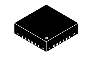
728-960 MHz, 1.6 W Avg., 28 V RF LDMOS Wideband Integrated Power Amplifier

  • \n Contact support,\n your local sales representative or an\n \n NXP Authorized Distributor\n \n for product availability.\n

See product image

Features

  • Characterized with Series Equivalent Large–Signal Impedance Parameters and Common Source S-Parameters
  • On-Chip Matching (50 Ohm Input, DC Blocked)
  • Integrated Quiescent Current Temperature Compensation with Enable/Disable Function
  • Integrated ESD Protection
  • RoHS Compliant
  • In Tape and Reel. T1 Suffix = 1,000 Units, 16 mm Tape Width, 13-inch Reel.

RF Performance Tables

800 MHz

Typical Single-Carrier W–CDMA Performance: VDD = 28 Volts, IDQ1 = 52 mA, IDQ2 = 134 mA, Pout = 1.6 Watts Avg., IQ Magnitude Clipping, Channel Bandwidth = 3.84 MHz, Input Signal PAR = 7.5 dB @ 0.01% Probability on CCDF.
Frequency Gps
(dB)
PAE
(%)
ACPR
(dBc)
865 MHz37.917.1–50.4
880 MHz38.017.4–50.6
895 MHz37.817.5–51.3
  • Capable of Handling 10:1 VSWR, @ 32 Vdc, 880 MHz, Pout = 23.5 Watts CW (3 dB Input Overdrive from Rated Pout)
  • Stable into a 5:1 VSWR. All Spurs Below –60 dBc @ 30 to 41.5 dBm CW Pout.
  • Typical Pout @ 1 dB Compression Point 15.5 Watts CW

700 MHz

Typical Single-Carrier W–CDMA Performance: VDD = 28 Volts, IDQ1 = 50 mA, IDQ2 = 144 mA, Pout = 1.6 Watts Avg., IQ Magnitude Clipping, Channel Bandwidth = 3.84 MHz, Input Signal PAR = 7.5 dB @ 0.01% Probability on CCDF.
Frequency Gps
(dB)
PAE
(%)
ACPR
(dBc)
728 MHz37.817.2–49.5
748 MHz37.817.3–50.5
768 MHz37.717.3–51.4

Buy/Parametrics


Documentation

Quick reference to our documentation types.

1-5 of 6 documents

Show All

Design Files

Quick reference to our design files types.

1-5 of 7 design files

Show All

Support

What do you need help with?