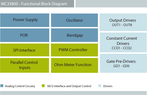
MC33800 | Engine Control Integrated Circuit | NXP Semiconductors

Engine Control Integrated Circuit

Roll over image to zoom in

Block Diagram

NXP MC33800 Low Side Switch Block Diagram

NXP MC33800 Low Side Switch Block Diagram

Features

Key Features

  • Wide operating voltage range, 5 < VPWR < 36 volts
  • Interfaces to 3.3 and 5 volt microprocessors via SPI protocol
  • Low, sleep mode, standby current, typically 10 uA.
  • Internal or external voltage reference
  • Internal oscillator with calibrate capability
  • Measures resistance to monitor HEGO sensors
  • CCDs have programmable current, dither frequency and amplitude
  • OSSs can be paralleled to increase current capability
  • GDs have programmable frequency and duty cycle PWM
  • All outputs controllable via serial and/or parallel inputs

Product Longevity Program

  • This product is included in the NXP Product Longevity Program ensuring a stable supply of products for your embedded designs. The MC33800 is included in the 15-year program

Buy/Parametrics


Documentation

Quick reference to our documentation types.

1-5 of 7 documents

Show All

Design Files

Hardware

Quick reference to our board types.

2 hardware offerings

Software

Quick reference to our software types.

1 software file

Note: For better experience, software downloads are recommended on desktop.

Engineering Services

4 engineering services

To find additional partner offerings that support this product, visit our Partner Marketplace.

Support

What do you need help with?