Design Files
Receive the full breakdown. See the product footprint and more in the eCad file.
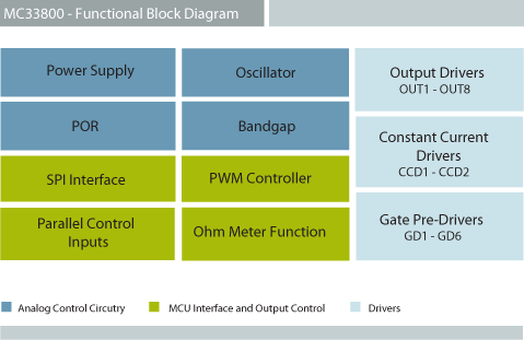
The NXP MC33800 is a combination output switch and driver IC that is ideal for numerous powertrain engine control applications.

Note: To see the product features close this window.
|
|
|
|
|
|
|
|---|---|---|---|---|---|
|
|
|
|
|
|
|
|
|
|
|
|
|
|
|
|
|
|
|
|
|
|
|
|
|
|
|
|
|
|
|
|
|
|
|
|
|
|
|
|
|
|
|
|
|
|
|
|
|
|
|
|
|
|
|
|
|
|
|
|
|
|
|
|
|
|
|
|
|
|
Quick reference to our documentation types.
1-5 of 7 documents
Please wait while your secure files are loading.
Receive the full breakdown. See the product footprint and more in the eCad file.

Receive the full breakdown. See the product footprint and more in the eCad file.
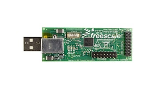
2 hardware offerings


Quick reference to our software types.
1 software file
Note: For better experience, software downloads are recommended on desktop.
Please wait while your secure files are loading.
2 engineering services


There are no results for this selection.
To find additional partner offerings that support this product, visit our Partner Marketplace.