Design Files

Receive the full breakdown. See the product footprint and more in the eCad file.
Sign in for a personalized NXP experience.
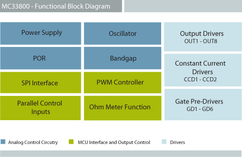
The NXP MC33800 is a combination output switch and driver IC that is ideal for numerous powertrain engine control applications.

Note: To see the product features close this window.
1 result
Include 0 NRND
Part | Order | CAD Model | Status | Device Function | Budgetary Price excluding tax | SafeAssure Functional Safety | Package Type | Package Termination Count | Load Current (IL) [TYP] (A) | Number of Channels | Drain-to-Source On Resistance (Typ) (mOhm) (RDS(ON)) | Load Supply Voltage (Min) (V) | Load Supply Voltage (Max) (V) | Supply Voltage [max] (V) | Supply Voltage [min] (V) | Interface and Input Control | Ambient Operating Temperature (Min to Max) (℃) |
|---|---|---|---|---|---|---|---|---|---|---|---|---|---|---|---|---|---|
Active | low side switch, powertrain control, pre-driver | 1K @ US$4.13 | No | HSOP54 | 54 | 0.35 | 1, 2, 6 | 250, 1000, 700000 | 5 | 36 | 5.5 | 3 | SPI / SPI | -40 to 125 |
Quick reference to our documentation types.
1-5 of 7 documents
There are no results for this selection.
Please wait while your secure files are loading.
1-5 of 7 documents

Receive the full breakdown. See the product footprint and more in the eCad file.
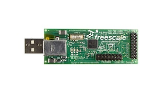
2 hardware offerings


2 hardware offerings


Quick reference to our software types.
1 software file
Note: For better experience, software downloads are recommended on desktop.
Please wait while your secure files are loading.
1 software file
Note: For better experience, software downloads are recommended on desktop.
4 engineering services


There are no results for this selection.
There are no results for this selection.
To find additional partner offerings that support this product, visit our Partner Marketplace.