- Analog Toolbox
- Getting Started with the P3S0210BQ-ARD
Getting Started with the P3S0210BQ-ARD
Contents of this document
-
Out of the Box
-
Get the Hardware
-
Configure the Hardware
Sign in to save your progress. Don't have an account? Create one.
Purchase your P3S0210 Bidirectional I3C-Bus Switch and Voltage Level Translator
1. Out of the Box
The NXP analog product development boards provide an easy-to-use platform for evaluating NXP products. The boards support a range of analog, mixed-signal and power solutions. They incorporate monolithic integrated circuits and system-in-package devices that use proven high-volume technology. NXP products offer longer battery life, a smaller form factor, reduced component counts, lower cost, and improved performance in powering state-of-the-art systems.
This page will guide you through the process of setting up and using the P3S0210BQ-ARD evaluation board.
2. Get to Know the Hardware
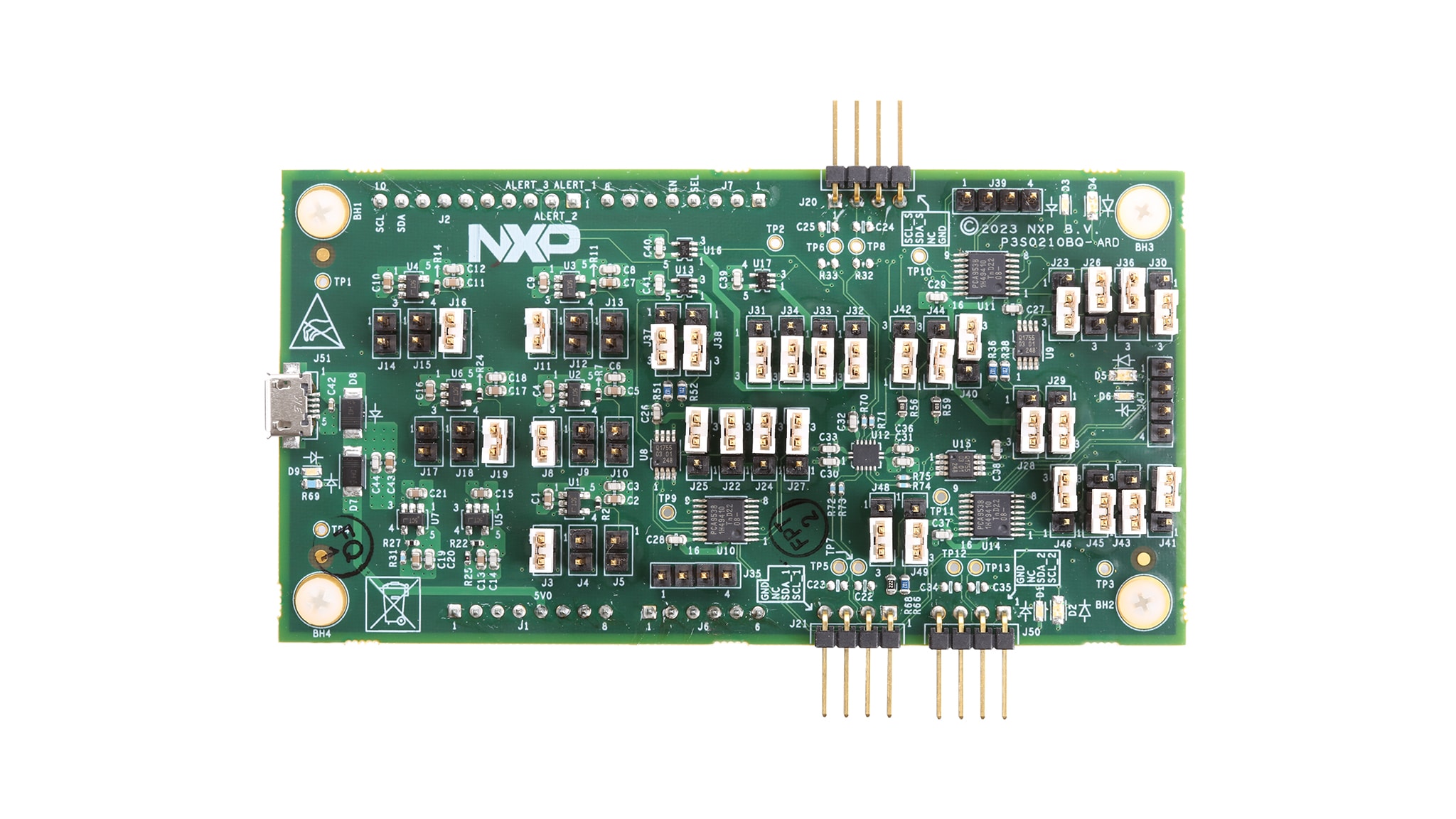
2.2 Board Description
The P3S0210BQ-ARD evaluation board is powered via a USB micro-B connector, J51. There are on-board LDOs to convert 5 V from the micro-B connector to other power rails to provide power to P3S0210 VCCP1, VCCP2, VCCS, VCCE, VCCR and other components on the board. The voltage at each LDO output can be selected via the headers at the LDO FB pin. The output voltage is set with a resistor divider, and a jumper is used to select the lower resistor to set the LDO output voltage.
Port 1 and Port 2 are preconfigured to 1.8 V and PortS is configured to 3.3 V. Other voltages can be selected to match a specific I3C controller/target via the on-board jumpers (see UM11909, P3S0210BQ-ARD Evaluation Board User Manual). It is strongly recommended that the board user manual should be read first before any attempt to use the board.
2.3 Board Components
P3S0210 VCCP1, VCCP2, VCCS, VCCE, VCCR Select Jumper Settings
As default, P3S0210 power rails are set as onboard power as shown in the next table. External power rail can be used by removing the jumper from 2-3, and placing it on 1-2
| Header | Jumper on | Comment |
|---|---|---|
JP31 |
1-2-3 | 1-2 external, 2-3 (default) onboard VCCP1 |
JP32 |
1-2-3 | 1-2 external, 2-3 (default) onboard VCCP1 |
JP33 |
1-2-3 | 1-2 external, 2-3 (default) onboard VCCP1 |
JP34 |
1-2-3 | 1-2 external, 2-3 (default) onboard VCCP1 |
JP40 |
1-2-3 | 1-2 external, 2-3 (default) onboard VCCP1 |
P3S0210 VCCP1, VCCP2, VCCS, VCCE, VCCR Default Voltage Jumper Settings
P3S0210 power rail voltages can be changed according to the following table
| Voltage Rail | Header | Jumper on | Comment |
|---|---|---|---|
VCCP1 J3 (1V8), J4 (1V2), J5 (1V0) J3 (default) VCCP1 is set to 1V8 |
J3 (1V8), J4 (1V2), J5 (1V0) |
J3 (default) |
VCCP1 is set to 1V8 |
VCCP2 J8 (1V8), J9 (1V2), J10 (1V0) J8 (default) VCCP2 is set to 1V8 |
J8 (1V8), J9 (1V2), J10 (1V0) |
J8 (default) |
VCCP2 is set to 1V8 |
VCCPS J14 (1V2), J15 (1V8), J16 (3V3) J16 (default) VCCS is set to 3V3 |
J14 (1V2), J15 (1V8), J16 (3V3) |
J16 (default) |
VCCS is set to 3V3 |
VCCR J17 (1V8), J18 (3V3), J19 (3V6) J19 (default) VCCR is set to 3V6 |
J17 (1V8), J18 (3V3), J19 (3V6) |
J19 (default) |
VCCR is set to 3V6 |
| VCCE | J11 (1V8), J12 (1V2), J13 (1V0) |
J11 (default) |
VCCE is set to 1V8 VCEE is set to 1V8 |
P3S0210 Enable and Switch Select Jumper Settings
P3S0210 enable and channel switch can be manually selected or be controlled by the external MCU via the Arduino extension headers.
| Pin | Header | Jumper on | Comment |
|---|---|---|---|
| OE | |
1-2-3 | 1-2 enable (default), 2-3 disable |
| SEL | J44 |
1-2-3 | 1-2 Port 2 connected PortS, 2-3 Port 1 connected PortS (default) |
On-board I²C and I³C Devices
The I2C and I3C addresses in the folloring table are the factory default addresses. These addresses can be changed to other addresses via headers. Please see the green footnotes on the P3S0210BQ-ARD evaluation board schematic.
| Type | Device | Port1 | Port2 | PortS |
|---|---|---|---|---|
| I2C | PCA9538 | U10 - Adr. 0xE0 | U14 - Adr. 0xE2 | U11 - Adr. 0xE4 |
| I3C | P3T1755 | U8 - Adr. 0x90 | U15 - Adr. 0x92 | U9 - Adr. 0x94 |
3. Configure the Hardware
3.1 Configure Hardware
- Unpack the board and power it with the USB2 cable
- Connect the external 1.8 V I3C controller to Port1 via
J21, or Port S via J20 of 3V3 I3C controller. - The I3C controller then can communicate with the 8-bit GPIO PCA9538 via I²C, or the temperature sensor P3T1755 via I3C on Port1. The 1.8 V I3C controller can also communicate with the 8-bit GPIO PCA9538 via I²C, or the temperature sensor P3T1755 via I3C on PortS as well. These devices are located at different I2C/I3C addresses.
Design Resources
Additional References
In addition to our P3S0210BQ: P3S0210BQ Dual Bidirectional I3C 1:2 Switch and VLT page, you may also want to visit: