Maintaining a lead in the shifting RF market requires continuous evolution,
and that’s something that we at NXP do very well. Using process technology to
create an edge, we’ve supported every generation of cellular and have
routinely set new standards for performance.
LDMOS technology is a classic example – having maintained a competitive
advantage for almost 30 years. They now enable the majority of the world’s
cellular voice and data traffic every day in some of the harshest
environments. NXP strives by anticipating change and optimizing for new
cellular requirements. Our latest
AirFast LDMOS technology
is helping drive cellular forward by supporting a global standard, including
LTE and 5G NR.
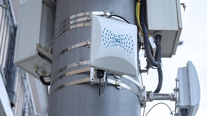
 5G repeater implemented on a city infrastructure pole
LDMOS is an ongoing technology and isn’t going anywhere anytime soon. LDMOS
still demonstrates high power and efficiency in cellular, broadcast and
narrowband applications – but it’s a mature technology that’s reaching the
limits of its ability.
Gallium Nitride (GaN), on the other hand, is a much younger technology and
shows great promise for future designs. See our
Versatile GaN Solution for Various Markets
device. GaN already performs with greater ease than LDMOS and offers room to
expand over time. In the 5G infrastructure, where base stations present a very
specific set of requirements, GaN becomes the clear choice for power
amplifiers (PAs), which are essential components for base stations.
The PA Challenge
In the signal chain of a cellular base station, the power amplifier (PA) sits
between the transmitter and the antenna. The PA takes the low-level RF signal
coming from the transmitter and boosts its power to the level required by the
antenna. Ideally, the PA boosts the signal without changing it, but
imperfections in the PA can add unwanted distortion to the signal and reduce
performance.
The PAs used for 5G need to do three things: They need to amplify signals to
higher frequencies than with previous generations of cellular, operate within
the same footprint, and they need to do this while using less energy.
LDMOS, which has been the go-to process technology for PAs for a long time,
does struggle to meet these three 5G requirements. GaN meets the challenge
head-on, with support for higher frequencies, lower power and smaller size.
Higher Frequencies
LDMOS works best at lower frequencies, especially below 3 GHz. For 5G, the
higher frequencies now being used GaN is more efficient. GaN can handle a
higher voltage in a much smaller area than comparable LDMOS devices and can
power a much wider range of mmWave frequencies than standard silicon. GaN is
already used for microwave transmission, which operates in an area of the
mmWave spectrum close to where new 5G use cases will be. GaN also supports
operation in the so-called C-band spectrum, between 3.7 and 4.2 GHz, which is
being opened up for 5G cellular operation.
Lower Power
Energy efficiency is a key issue for power amplifiers. Base stations are some
of the most energy-intensive pieces of equipment in the cellular network, and
as much as 20% of the electricity used by a base station can be attributed to
the PA. As a result, even small increases in efficiency can lower annual
electricity bills and reduce the CO2 footprint of cellular communications.
Higher data rates and increased bandwidth increase power consumption, so each
successive generation of cellular has needed more energy to run. This is
especially true with 5G. According to a 2019 report from ABI Research, a
typical 4G LTE cell site consumes somewhere between 6 and 9 kW, depending on
the level of traffic (periods of high traffic consume more power). ABI
estimates that a typical 5G base station, which will support 2G, 3G and 4G
traffic, as well as 5G traffic operating in different bands between 700 MHz
and 3.5 GHz, is likely to draw as much as 14 kW on average and up to 19 kW
during peak load. Add to this the fact that achieving full 5G coverage will
involve deploying many more small-cell base stations, and the amount of power
required to support 5G goes up even more.
Smaller Size
To make the transition to 5G more cost-effective, the goal is to develop 5G
solutions that fit in the same footprint used by present-day 4G solutions.
This makes 5G’s functionality easier to deploy and less disruptive because
this solution fits in the same space provided by the enclosure and more of the
base station’s equipment can remain in place.
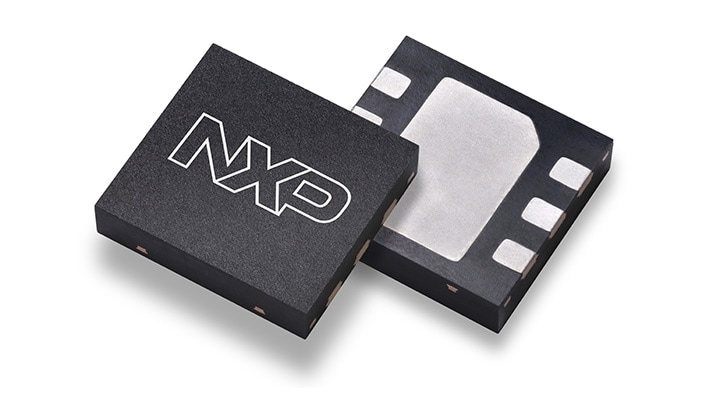
 Compact DFN 7 x 6.5 mm over-molded plastic package for optimal thermal
performance
GaN supports high-frequency operation, with higher power density and higher
efficiency than LDMOS. However, GaN does all this in a thermal package
comparable to that used by LDMOS technology. Also, since one GaN device can
support multiple bands, a single device can be used to cover a broader range
of use cases, and lowers the overall cost of the deployment.
NXP’s Continued Big Investment in GaN for 5G
We’ve been involved with GaN since 2003, and now offer a
complete
portfolio optimized for cellular infrastructure operation. Our 48 V GaN
discretely delivers high power density in a small footprint and supports
multiband operation, high-frequency capability and high efficiency. A prime
example is our versatile device –
the A3G26D055N
– a GaN solution that has an unmatched output to fill multiple frequency bands
and can be used across various markets.
We believe that our recent decision to bring our GaN process in-house
positions us for continued leadership in power amplifiers. Our new,
state-of-the-art six-inch (150 mm) RF GaN fab in the United States is built
specifically to support the needs of 5G operation. Our process experts in
Chandler, Arizona, have optimized the GaN technology to meet customer
requirements and simplify the interaction between the RF and digital-control
portions of the design. Also, the Chandler GaN facility is the only one in the
United States today that adheres to strict automotive quality standards for an
added level of reassurance for 5G operation.
 NXP’s GaN Fab clean room showing one of many bays with equipment and exhaust
pipes
The Chandler GaN facility continues to enable close collaboration between the
fab and the R&D team. This collaboration has helped expand our portfolio
across all frequencies and power levels. Carefully planned upgrades and
rollouts are expected to deliver even higher levels of efficiency, size and
cost, with a focus on the delivery of linearized RF performance.
Our work in Chandler underscores our commitment to 5G and is another example
of how we continue to build on our track record of leadership in RF process
technology.
To learn more about the Chandler GaN fab and our continued work in 5G, visit
www.nxp.com/RFGaN.
Check out our latest
design resources
on the web. NXP has implemented its own user interactive product guide, the RF
Product Selection Assistant. NXP is giving customers the capability to browse
our Macro RRH, active antenna systems and our industrial and consumer
portfolios.


