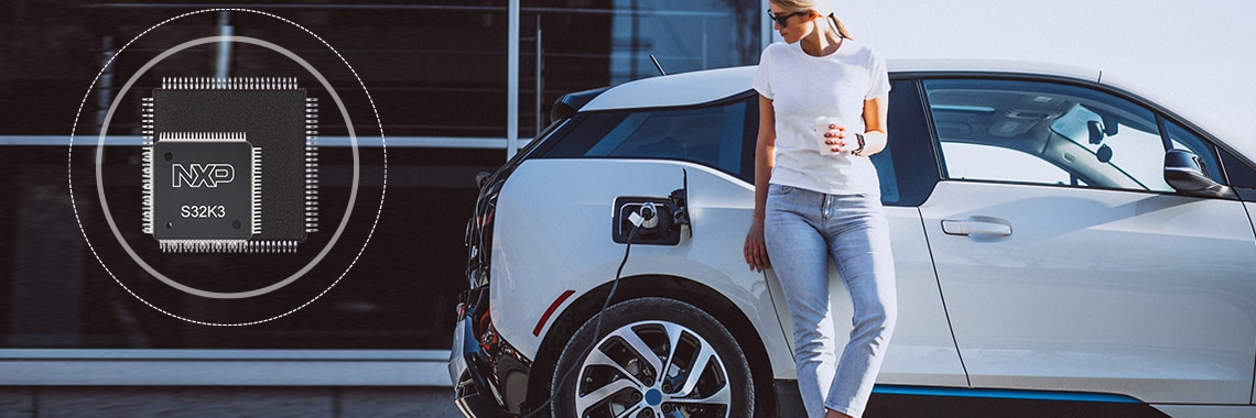
The High Density Quad Flat Package (HDQFP) is an innovative IC package developed by our engineering team in
Tianjin, intended to simplify packaging portfolios by offering greater lead
density over the well-known QFP.
Integrated circuit (IC) packaging is all about encasing a semiconductor
die and providing the connection from the electrical contacts of the die to
the connection on a printed circuit board (PCB). The IC dies are fabricated
from semiconductor wafers layered in a complex formation with copper and other
materials. The wafers are tested and singulated into an individual die which
is then packaged. IC packaging is
as crucial as the IC itself as packages help
transform bare ICs into actual functional products. The package serves four
purposes: to protect from physical damage, preserve from corrosion, help
dissipate heat, and most importantly, connect the electrical contacts on the
semiconductor device to the external environment, such as the PCB. System
engineers invest considerable time selecting an adequate package for each
application, not only assessing the package capability and reliability but
also balancing its affordability with performance.
Packaging technologies including package designs and architectures, materials,
processes and manufacturing equipment must evolve to respond to market
demands for cost-effective miniaturization. Innovation in such mature package
technology as quad flat package (QFP) is difficult yet has happened.
Innovation of High Density Quad Flat Package (HDQFP)
The ultra-reliable quad flat package (QFP) has been a go-to package for many
years. QFP continues to offer considerable benefits for engineers and their
designs: cost-effectively delivering mechanical, thermal and reliability
performance, along with the optical inspection. However, its downside has been
its footprint, especially with the increasing I/Os required in today's
microcontrollers. Gaining more I/Os needs significant area growth in the
package, leading engineers to choose area-array packages instead of QFP—like
ball grid array (BGA), array quad flat no-leads (QFN) or other versions of a
denser QFP with QFN-like leads tucked underneath.
An engineering team in our assembly facility in Tianjin, China (NXP-ATTJ)
proposed a new package that significantly shrinks the size of a QFP while
maximizing the number of I/Os on the package periphery: the HDQFP package.
 The original inspiration came from Bai Zhigang and Yao Jinzhong, along with
Pang Zingshow, Xu Xueson, Mao Chao, Li Jun, and Stephen Lee.
Their basic idea was to combine the gull-wing leads of a QFP with the J-leads
of a plastic leaded chip carrier (PLCC) in two interstitial tiers of leads
extending from the package body. With this configuration, HDQFP effectively
doubles the number of leads on the package periphery. Because the formed from the individual lead type to the PCB is
optically inspectable, all
HDQFP leads are optically inspectable.
Having a new package design is not where the process ends: many design and
process iterations, numerous routing requirements and board analysis, mold
bleed issues, new equipment requirements, wire bond reliability, lead frame
costs, die tolerances, manufacturability and yield. Nevertheless, all
challenges were bravely addressed and resolved along with years of engineering
inspiration and perspiration from the initial group in Tianjin to people from
NXP's development, manufacturing, test, product, marketing and sales teams
across the world as well as our lead frame and equipment suppliers.
HDQFP Offers Many Advantages Over QFP
- High I/O density: Combined PLCC J-leads and QFP gull-wing leads
-
Full inspectability: All leads are fully inspectable, demonstrating our
commitment to Total Quality by continuing our journey toward zero defects
- Automotive reliability: Target automotive and industrial applications
-
Reduced footprint: Package footprint on PCB can be reduced by 47% resulting
in cost savings for customers
-
Simplify package portfolio: Reduce five QFP body sizes to two HDQFP sizes
-
No extra cost to PCB: HDQFP uses the same PCB line/space design as 0.5 mm
pitch LQFP
-
Excellent solder joint reliability: First fail occurred at 9700 cycles
- Component level reliability: Exceed 2x AEC Grade 1
- Equivalent thermal and electrical performance to QFP
 A visual comparison between 172 HDQFP (16x16) and 176 LQFP (24x24) showing
the body size reduction up to 55%.
HDQFP is the result of NXP’s global expertise and engagement of many to make
it a reality from deep technical know-how to market insight, strong customer
relationships and extensive customer assistance. Volume manufacturing is now
beginning. Learn more about
HDQFP.
You can read Chip Scale Review’s
Emerging Technologies
column
(pages 12-18, September/October 2021) describing in detail the genesis of the
HDQFP package and the engineering team's quest to find a better packaging
solution that also accommodates the drive to zero defects for automotive
applications or the
Technical
article
(pages 18-24, November/December 2021) including a technical data summary about
HDQFP's evaluation by reliability testing, construction analysis,
inspectability evaluation and mechanical, thermal and electrical simulation.
HDQFP has been presented at the
2021 IEEE 23rd Electronics
Packaging Technology Conference (EPTC); also, in both iMAPS' 17th international conference on
Device Packaging
and the 54th international symposium on microelectronics.
HDQFP will also be featured at the upcoming
2022 IEEE 72nd Electronic Components and Technology
Conference (ECTC).
S32K3 Is the First
The S32K3 microcontroller family (the latest addition to our S32K product
line) is the first NXP MCU to offer the breakthrough HDQFP package,
increasing I/O density while meeting the demanding requirements for automotive
applications. S32K3 MCU is currently offered in 100 10x10mm HDQFP and 172
16x16 mm HDQFP with and without an exposed pad.
Read more at
NXP Tackles Cost and Complexity of
Automotive Software Development with New
S32K3 MCUs.


