Electrification of passenger and commercial vehicles has brought about
significant changes to the R&D process of various sub-systems in the
automotive and e-mobility market. Primarily, the fast pace in moving from
design concept to market readiness of EV systems is unusual in a “traditional”
automotive development cycle.
Furthermore, in comparison to ICE systems (engines and transmission), these
relatively “simpler” EV systems have enabled the entrance of non-traditional
Tier 1 suppliers to the automotive ecosystem, thus increasing competition. To
combat the impact of rising costs and maintain control of IP and the bill of
materials (BOM), many OEMs are moving towards building in-house capability to
design, develop and manufacture these subsystems. Meanwhile, the traditional
Tier 1s continue to invest in EV systems whilst competing with new entrants
and trying to maintain their penetration with the OEMs. In order to maintain
relevancy and provide differentiated services, some Tier 1 suppliers offer to
integrate multiple pieces of key EV system components, like inverter, traction
motor and gear-box. OEMs and new Tier 1 suppliers both face a steep learning
curve with regards to the system analysis and integration, especially related
to functional safety requirements. As a consequence, they increasingly look
towards their semiconductor suppliers to help close this development and
knowledge gap.
The different automotive sub-systems have varying demands with regards to
system performance and functional safety. In the specific case of traction
inverter systems, the trend is to increase features to achieve maximum
efficiency and reduced BOM cost. High performance intelligent gate drivers are
starting to emerge to meet the demands for increased features and performance
while reducing board area and BOM cost.
Newer gate drivers, like NXP’s
GD3100
and
GD3160, provide intelligence and programmability which not only protect the SiC or
IGBT power devices in the face of harsh operating conditions, but also
increase system efficiency and reduce fault detection/ reaction times.
 GD3160 block diagram
Integrated high-voltage (> 1,000 Vrms) isolation allows for the
digital reporting of various types of information, from the high voltage (400
V to 800 V) domain to the low voltage (12 V) domain. These parameters include
various fault conditions, power device temperature and VCE or VGE state of
the power device. Improved monitoring of these various parameters aid in
achieving ASIL D functional safety of the EV system. Gate drive wave-shaping
features such as the segmented drive allow customers to optimize switching for
efficiency while protecting against overshoot, which translates to lower EMC
noise.
Want to know more about the GD3160? Read our latest
fact sheet.
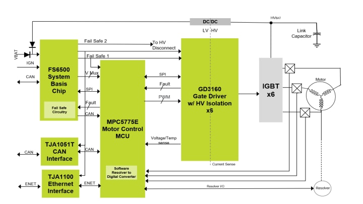
 Traction inverter system block diagram
At NXP, we stay committed to providing system solutions such as
traction inverter reference designs
and
full inverter evaluation tools
along with the functional safety documentation to enable reduced development
cost and faster time to market.
For more information, please see our video about
NXP isolated gate driver features and benefits
video.


