
Application Note (8)
-
UUencoding for UART ISP[AN11229]
-
Using the LPC32xx VFP[AN10902]
-
LPC32x0 power supply design examples[AN10777]
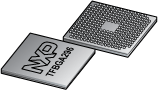
The LPC3250 operates at CPU frequencies of up to 266 MHz. The NXP® implementation uses an ARM926EJ-S CPU core with a Harvard architectur, 5-stage pipeline, and an integral Memory Management Unit. The LPC3250 also includes 256 kB of on-chip static RAM, a NAND flash interface, an Ethernet MAC, an LCD controller that supports STN and TFT panels, and an external bus interface that supports SDR and DDR SDRAM, as well as static devices. In addition, the LPC3250 includes a USB 2.0 full-speed interface, seven UARTs, two I2C-bus interfaces, two SPI/SSP ports, two I2S-bus interfaces, two single output PWMs, a motor control PWM, six general purpose timers with capture inputs and compare outputs, a Secure Digital interface, and a 10-bit Analog-to-Digital Converter with a touch screen sense option.
| | | | | |
|---|---|---|---|---|---|
| | | | | |
| | | | | |
| | | | | |
| | | | | |
| | | | | |
| | | | | |
| | | | | |
| | | | | |
| | | | | |
| | | | | |
Quick reference to our documentation types.
1-10 of 13 documents
Compact List
1-10 of 13 documents
Compact List
4 design files
4 hardware offerings
To find additional partner offerings that support this product, visit our Partner Marketplace.
Quick reference to our software types.
1-5 of 21 software files
To find additional partner offerings that support this product, visit our Partner Marketplace.
To get further assistance directly from NXP, please see our Engineering Services.
1-5 of 10 engineering services


To find additional partner offerings that support this product, visit our Partner Marketplace.
5 trainings
To find additional partner offerings that support this product, visit our Partner Marketplace.
There are no recently viewed products to display.
