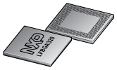
The LPC3180 is an ARM9-based microcontroller for embedded applications requiring high performance combined with low power dissipation. It achieves these objectives through the combination of NXP®'s state-of-the-art 90 nanometer technology with an ARM926EJ-S CPU core with a Vector Floating Point (VFP) coprocessor and a large array of standard peripherals including USB On-The-Go.
The microcontroller can operate at over 200 MHz CPU frequency (about 220 MIPS per Arm Inc.). The ARM926EJ-S CPU incorporates a 5-stage pipeline and has a Harvard architecture with separate 32 kB instruction and data caches, a demand paged MMU, DSP instruction extensions with a single cycle MAC, and Jazelle Java bytecode execution hardware. A block diagram of the microcontroller is shown .
Power optimization in this microcontroller is done through process and technology development (Intrinsic Power), and architectural means (Managed Power).
The LPC3180 also incorporates an SDRAM interface, NAND flash interfaces, USB 2.0 full-speed interface, seven UARTs, two I²C-bus interfaces, two SPI ports, a Secure Digital (SD) interface, and a 10-bit ADC in addition to many other features.


