Getting Started with the UJA1168AXF Evaluation Board
Contents of this document
-
Get Started
-
Get to Know the Hardware
-
Configure Hardware
Sign in to save your progress. Don't have an account? Create one.
Purchase your UJA1168A
1. Get Started
The NXP analog product development boards provide an easy-to-use platform for evaluating NXP products. The boards support a range of analog, mixed-signal and power solutions. They incorporate monolithic integrated circuits and system-in-package devices that use proven high-volume technology. NXP products offer longer battery life, a smaller form factor, reduced component counts, lower cost, and improved performance in powering state-of-the-art systems.
This page will guide you through the process of setting up and using the UJA1168AXFEVB evaluation board.
1.1 Kit Contents/Packing List
The UJA1168AXF-EVB contents include:
- Assembled and tested evaluation board in an antistatic bag
1.2 Additional Hardware
In addition to the kit contents, the following hardware is necessary or beneficial when working with this kit.
- Power supply with a 12 V DC source and a current limit capability of at least 1.0 A
- A 5.0 V MCU board that contains at least one CAN/CAN FD controller and one SPI master
2. Get to Know the Hardware
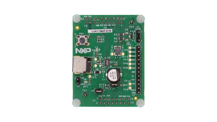
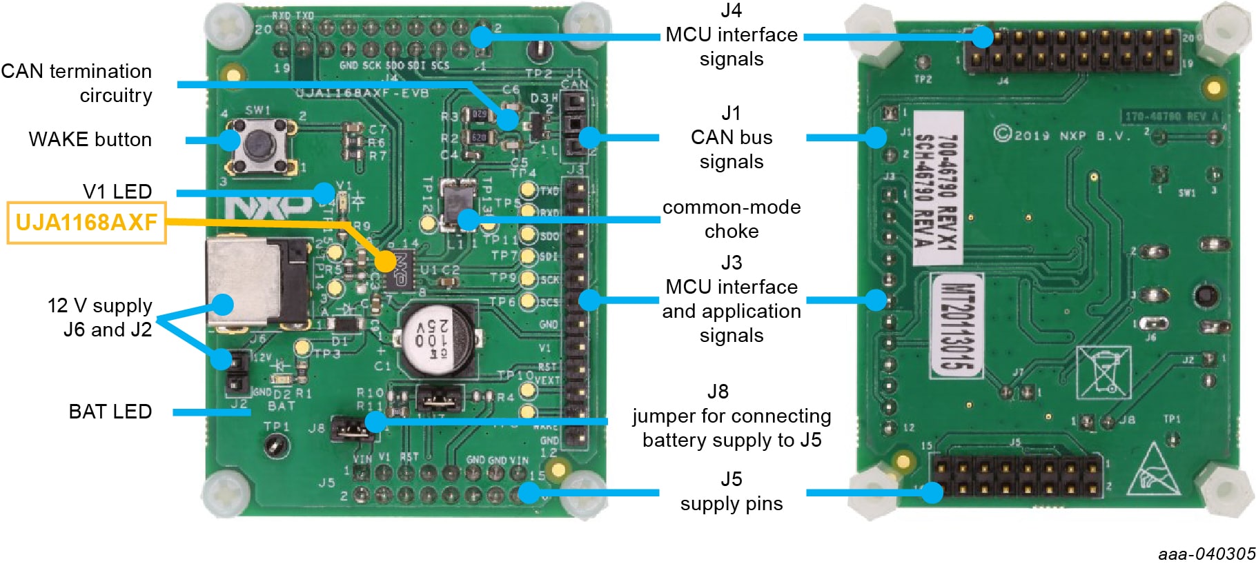
2.1 Board Description
The UJA1168AXF-EVB evaluation boards are designed to facilitate the testing and evaluation of UJA1168AXF product features in a variety of microcontroller IO interface environments. All MCU interface signals can be accessed in two ways: at a header row on the top side and also at header rows on the bottom side that can be plugged directly into many NXP MCU evaluation boards.
The UJA1168AXF-EVB evaluation boards are designed to be compatible with the S32K1xx evaluation board series from NXP and to support the use of standard software development tools and drivers.
2.2 Board Components
Board dimensions are 45.1 mm × 58.4 mm. Only components needed to support basic UJA1168AXF functionality are included. All boards contain circuitry for reverse polarity protected battery supply, BAT and V1 signal status LEDs, and CAN bus termination. Wake-up circuitry is also included since the UJA1168AXF device supports sleep mode. The board also provides several header rows (2.54 mm pitch) for connecting MCU interface and application signals.
3. Configure Hardware
3.1 Configure Hardware
To connect the UJA1168AXF-EVB to a CAN network, complete the following procedure.
The following conditions must be met before powering up the system with a 12 V supply:
- Connect boards in the ECU to a common GND
-
Connect SPI pins to the MCU SPI controller:
- SDO (
J3-03,J4-09) → MISO - SDI (
J3-04,J4-07) → MOSI - SCK (
J3-05,J4-11) → SCK - SCSN (
J3-06,J4-05) → CS
- SDO (
- Connect TXD/RXD (
J3-01/J3-02,J4-18/J4-20) pins to the MCU CAN controller TXD/RXD pins - Connect RSTN (
J9-09/J5-05) to the MCU reset pin - Connect CANH and CANL (
J1-01/J1-02) to the CAN bus twisted pair cables - Connect V1 (
J3-08,J5-03) to the MCU supply unit - Connect INH (
J3-10) on the UJA1168AF-EVB to the control/enable pin on the ECU supply unit (optional)
Once the above steps have been completed, the ECU/EVB can be powered up using an external battery supply. The UJA1168AXF-EVB starts up in Forced Normal mode (if MTP is not configured) or Standby mode (if MTP configured), awaiting commands from the MCU via the SPI interface.