Getting Started with the PCA9451A-EVK Evaluation Board
Contents of this document
-
Out of the Box
-
Get Hardware
-
Configure Hardware
Sign in to save your progress. Don't have an account? Create one.
Purchase your PCA9451A-EVK
1. Out of the Box
The NXP analog product development boards provide an easy-to-use platform for evaluating NXP products. The boards support a range of analog, mixed-signal and power solutions. They incorporate monolithic integrated circuits and system-in-package devices that use proven high-volume technology. NXP products offer longer battery life, a smaller form factor, reduced component counts, lower cost and improved performance in powering state-of-the-art systems.
This page will guide you through the process of setting up and using the PCA9451A-EVK board.
1.1 Kit Contents and Packing List
The PCA9451A-EVK kit contents include:
- 1x PCA9451A evaluation board, which allows easy evaluation on function and features
- 1x Interface cable, which serves as a USB to I²C interface between the computer and the PCA9451A evaluation board
1.2 Additional Hardware
In addition to the kit contents, the following hardware is necessary or beneficial when working with this kit.
- Power supply with a range of 3.0 V to 5.0 V and a current limit set initially to 1.0 A (maximum current consumption can be up to 7.0 A)
- Oscilloscope/multimeter
- Electronic load (optional) - each power rail output can be connected to e-load for testing
1.3 Windows PC Workstation
This evaluation board requires a Windows PC workstation. Meeting these minimum specifications should produce great results when working with this evaluation board:
- USB-enabled computer with Windows 7, Windows 8, or Windows 10
1.4 Software
Installing software is necessary to work with this evaluation board.
- Go to PCA9451A Evaluation Board
- Extract the zip file PCA9451_EVB_GUI.zip into selected folder. No need to install (if password is asked during unzip, then type “NXP”)
- Install the FTDI cable driver from here
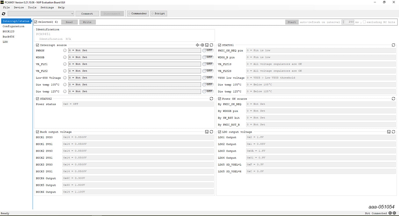
- Run the file PCA9451.exe. The interface window is shown in Figure 1
2. Get Hardware
2.1 Board Features
- Six buck regulators
- One 4.0 A dual-phase buck regulator with DVS
- One 2.0 A buck regulator with DVS
- One 3.0 A buck regulator
- One 2.0 A buck regulator
- One 1.5 A buck regulator
- Three linear regulators
- One 10 mA LDO
- One 150 mA LDO
- One 200 mA LDO
- 400 mA load switch with a built-in active discharge resistor
- 32.768 kHz crystal oscillator driver and buffer output
- Two-channel logic level translator
- System features
- 2.85 V to 5.5 V operating input voltage range
- Power ON/OFF control
- Standby/run mode control
- Smart DVS control
- Interrupt configuration
- Fm+ 1 MHz I²C Interface (via FTDI USB to I²C cable)
2.2 Board Description
This evaluation board features the PCA9451A power management IC. The kit integrates all hardware needed to fully evaluate the PMIC. It integrates a communication bridge based on FTDI to interface with the PCA9451A GUI software interface to fully configure and control the PMIC.
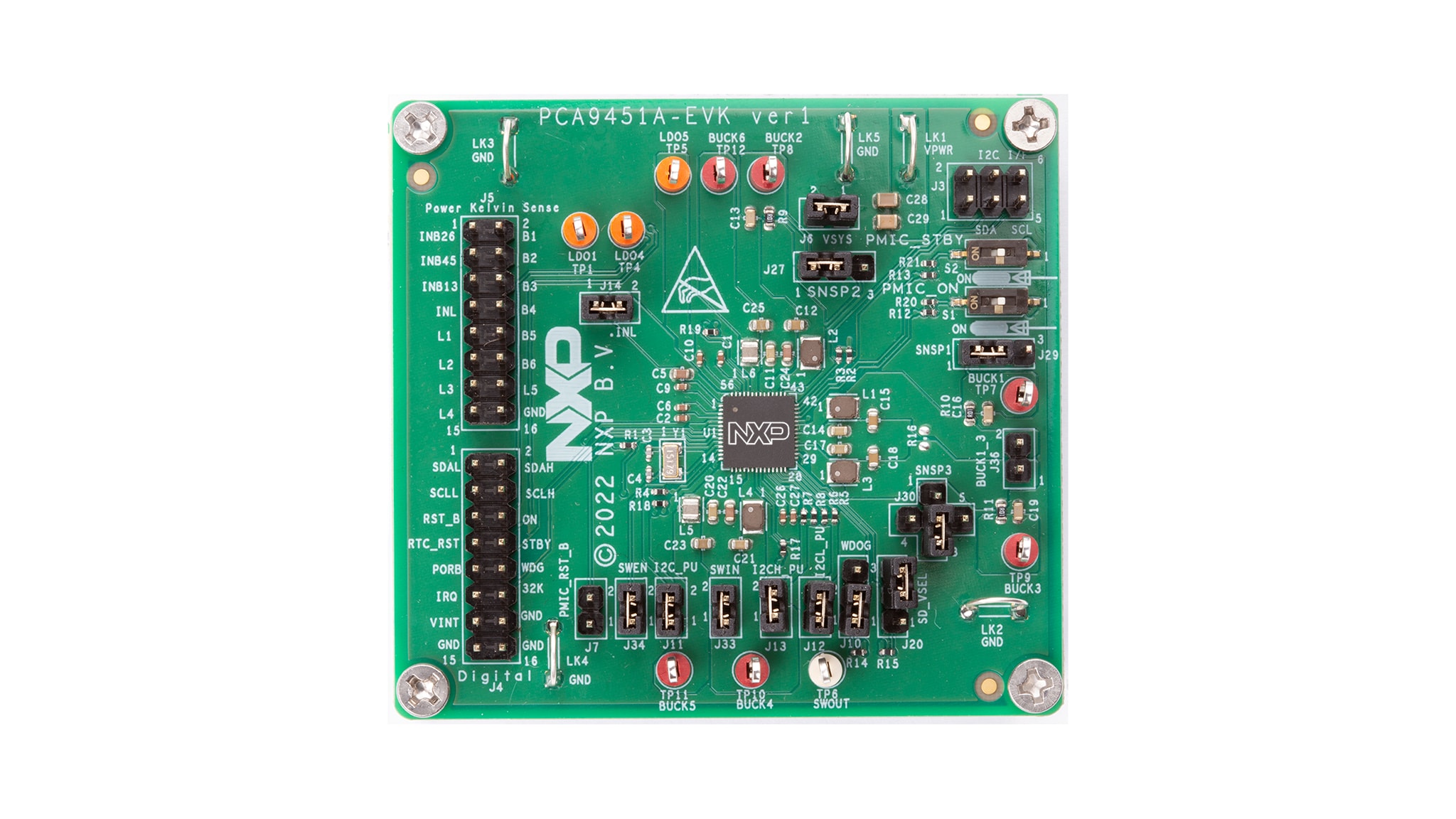
2.3 Board Components
Overview of the PCA9451A-EVK board
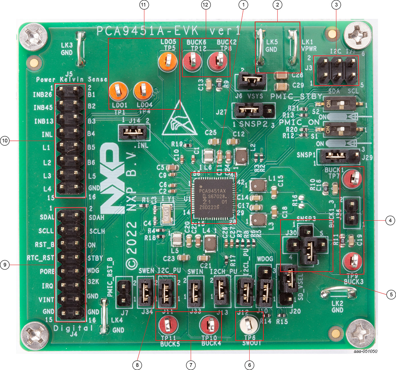
- PCA9451A PMIC
- VPWR and GND input power connectors
- I²C connector
- BUCK1 and BUCK3 output test points
- BUCK3 feedback connection
- Load switch output test point
- BUCK4 and BUCK5 output test points
- I²C pullup voltage jumper (I²C_PU)
- Digital IO connector
- Kelvin sense connector
- LDO outputs test points
- BUCK2 and BUCK6 output test points
3. Configure Hardware
3.1 Configure Hardware
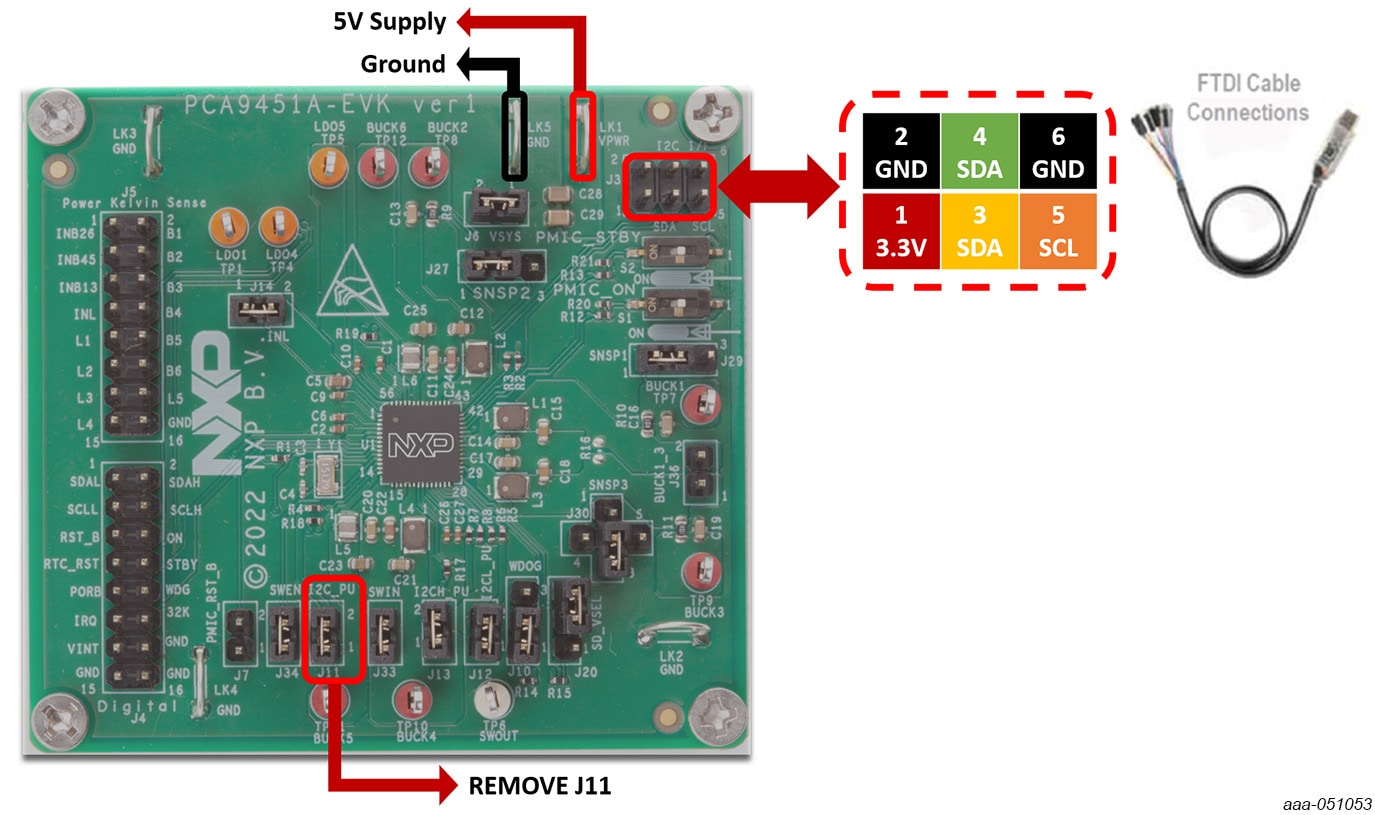
Connect the wires of the FTDI cable on the following pins as shown in Figure 3, and make sure the power supply is turned off and the USB connector is disconnected during the wiring stage:
- Connect both SDAs, SCL, GND, and the 3.3 V wires from the FTDI cable
- SCL serial clock signal (orange cable) should be connected to pin 5 of the ‘Digital IO’ connector (
J3). - Both SDA serial data wires (yellow and green cables) should be connected to create bidirectional data. Connect yellow cable to pin 3, and green cable to pin 4 of the ‘Digital IO’ connector (
J3) - GND ground signal (black cable) should be connected to pin 6 or pin 2 of the ‘Digital IO’ connector (
J3) - Remove jumper from
J11 - 3.3 V supply wire (red cable) from FTDI cable should be connected to pin 1 of the ‘I²C connector’ (
J3)
- SCL serial clock signal (orange cable) should be connected to pin 5 of the ‘Digital IO’ connector (
- With the power supply turned off, connect 5.0 V power supply to LK1 connector and corresponding ground to LK5
- Turn ON power supply
- Connect USB connector of the FDTI cable to PC
- Set switch S1 to "ON" position
Note:
- Make sure
J30is set to 2-5 for dual-phase configuration. Some boards are configured withJ30= 2-3 by default - Some boards are configured with
J36open by default. Make sureJ36is set to 1-2 for dual-phase configuration